Method for forming coating film on facet of semiconductor optical device

Inactive Publication Date: 2012-08-23
SUMITOMO ELECTRIC IND LTD
View PDF4 Cites 0 Cited by
  • Summary
  • Abstract
  • Description
  • Claims
  • Application Information

AI Technical Summary

Benefits of technology

[0017]Furthermore, in the aforementioned method for forming a coating film on a facet of a semiconductor optical device, the LD bar may have a width smaller than or equal to 200 μm in a direction perpendicular to the second direction. When the LD bars have a relatively small width, the spacers need to be reduced in thickness, causing the spacers to deform e

Problems solved by technology

However, the above-described coating-film forming method has the follow

Method used


Image

  • Method for forming coating film on facet of semiconductor optical device
  • Method for forming coating film on facet of semiconductor optical device
  • Method for forming coating film on facet of semiconductor optical device

Examples


Embodiment Construction

[0041]A method for forming a coating film on a facet of a semiconductor optical device according to an embodiment of the present invention will now be described in detail with reference to the attached drawings. In the drawings, the same components are given the same reference numerals, and redundant descriptions thereof will be omitted.

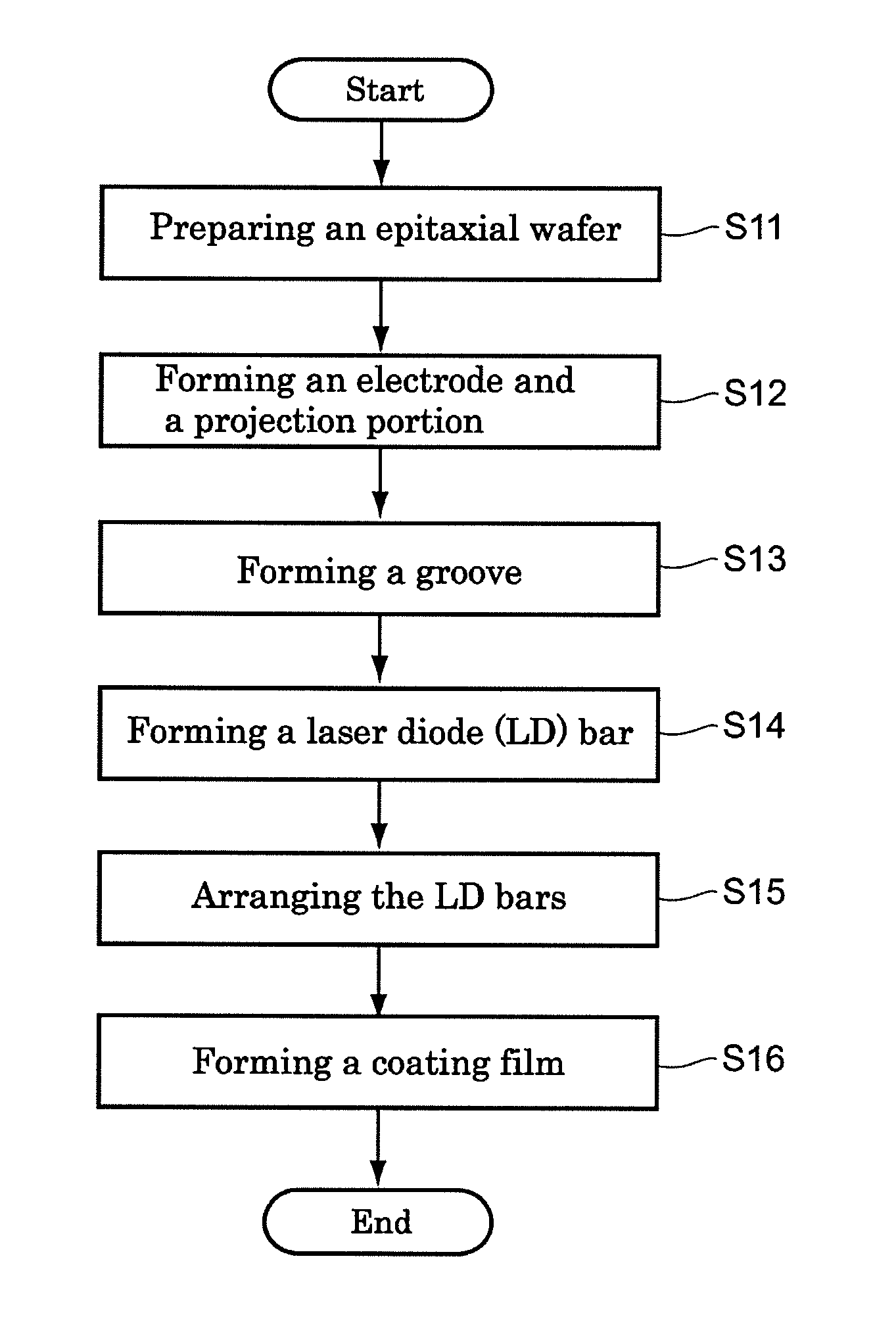
[0042]FIG. 1 is a flowchart showing the method for forming a coating film on a facet of a semiconductor optical device according to this embodiment. In this embodiment, the method for forming a coating film on a facet of a semiconductor laser as a semiconductor optical device is described. FIGS. 2 to 15 are diagrams for explaining the steps included in the method for forming the coating film on the facet of the semiconductor laser according to this embodiment. In FIGS. 3 to 12B, an XYZ orthogonal coordinate system is illustrated to provide an easier understanding of the description.

[Preparation of Epitaxial Wafer]

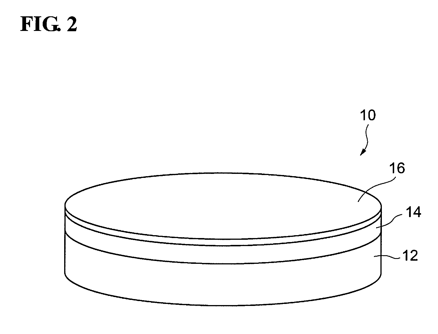
[0043]First, in step S11, an epitaxia...


PUM


Abstract

The method includes the steps of preparing an epitaxial wafer by forming a multilayer semiconductor structure on a main surface of a substrate; forming stripe electrodes and bonding pads on the multilayer semiconductor structure with the bonding pads being respectively electrically connected to the stripe electrodes; forming a projection portion on the multilayer semiconductor structure; forming laser diode (LD) bars by cutting the epitaxial wafer; arranging the LD bars on a support surface such that a side surface thereof is oriented normal to the support surface, and disposing spacers between the LD bars; and forming a coating film on the side surface. The projection portion has a height, measured from the main surface of the substrate, greater than a height of the stripe electrodes. Furthermore, the laser diode bar has at least one projection portion.

Description

BACKGROUND OF THE INVENTION[0001]1. Field of the Invention[0002]The present invention relates to a method for forming a coating film on a facet of a semiconductor optical device.[0003]2. Description of the Related Art[0004]Japanese Unexamined Patent Application Publication No. 2007-123374 discusses a method for forming a coating film on an end facet of a laser diode (LD) bar. In the coating-film forming method discussed in this document, a multilayer semiconductor structure including an active layer is first formed on a semiconductor substrate. Next, the semiconductor substrate is cleaved so that LD bars are formed. Subsequently, the LD bars are arranged with their cleaved facets facing upward, and spacers are disposed between the neighboring LD bars. Then, a coating film is formed on the cleaved facet of each LD bar. The thickness of each spacer is smaller than or equal to the width of each LD bar in the direction perpendicular to the cleaved facet.SUMMARY OF THE INVENTION[0005]For...

Claims


Application Information

Patent Timeline
IPC IPC(8): H01L33/08H01S5/02375
CPCH01S5/0202H01S5/0425H01S5/028H01S5/02268H01S5/04256H01S5/04252H01S5/02375
Inventor ONISHI, YUTAKA
Owner SUMITOMO ELECTRIC IND LTD
Why Eureka
Try Eureka