Treatment solution for preventing pattern collapse in metal fine structure body, and process for production of metal fine structure body using same
a fine structure body and treatment solution technology, applied in the direction of detergent compositions, chemical instruments and processes, organic chemistry, etc., can solve the problems of pattern collapse, no effective measure to prevent and the pattern collapse of the structure is becoming a major problem, so as to achieve the effect of suppressing the pattern collapse and producing a fine metal structur
- Summary
- Abstract
- Description
- Claims
- Application Information
AI Technical Summary
Benefits of technology
Problems solved by technology
Method used
Image
Examples
example
[0035]The present invention will be described in more detail with reference to examples and comparative examples below, but the present invention is not limited to the examples.
Preparation of Processing Liquid
[0036]Processing liquids for suppressing pattern collapse of a fine metal structure were prepared according the formulation compositions (% by mass) shown in Table 1. The balance is water.
TABLE 1KindContentProcessing liquid 1Surfron S-221 *150%Processing liquid 2Surfron S-221 *1 2%Processing liquid 3Surfron S-221 *11,000ppmProcessing liquid 4Surfron S-231 *220%Processing liquid 5Surfron S-231 *21ppmProcessing liquid 6Surfron S-231 *210ppmProcessing liquid 7Surfron S-241 *310%Processing liquid 8Surfron S-241 *3 1%Processing liquid 9Surfron S-241 *350ppm*1 “Surfron S-221 (trade name), produced by AGC Seimi Chemical Co., Ltd., perfluoroalkyltrialkylammonium halide*2 “Surfron S-231 (trade name), produced by AGC Seimi Chemical Co., Ltd., perfluoroalkyl betaine*3 “Surfron S-241 (trad...
examples 1 to 9
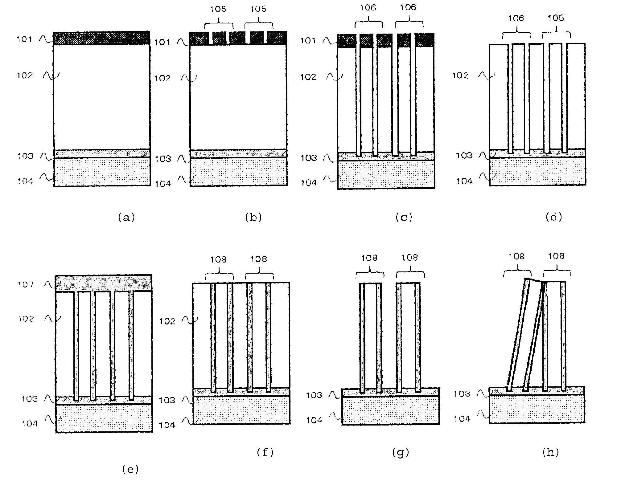
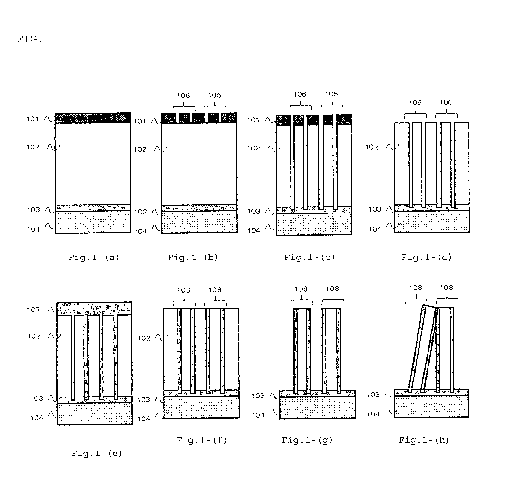
[0037]As shown in FIG. 1(a), silicon nitride 103 (thickness: 100 nm) and silicon oxide 102 (thickness: 1,200 nm) were formed as films on a silicon substrate 104, then a photoresist 101 was formed, and the photoresist 101 was exposed and developed, thereby forming a circular and ring-shaped opening 105 (diameter: 125 nm, distance between circles: 50 nm), as shown in FIG. 1(b). The silicon oxide 102 was etched by dry etching with the photoresist 101 as a mask, thereby forming a cylindrical hole 106 reaching the layer of silicon nitride 103, as shown in FIG. 1(c). The photoresist 101 was then removed by ashing, thereby providing a structure having the silicon oxide 102 with the cylindrical hole 106 reaching the layer of silicon nitride 103, as shown in FIG. 1(d). The cylindrical hole 106 of the resulting structure was filled with tungsten as a metal 107 (FIG. 1(e)), and an excessive portion of the metal (tungsten) 107 was removed by chemical mechanical polishing (CMP), thereby providin...
examples 10 to 18
[0042]Structures shown in FIG. 1(g) were obtained in the same manner as in Examples 1 to 9 except that titanium nitride was used as the metal 107 instead of tungsten. The resulting structures had a fine structure with a pattern containing cylindrical hollows 108 of the metal (titanium nitride) (diameter: 125 nm, height: 1,200 nm (aspect ratio: 9.6), distance between the cylindrical hollows: 50 nm), and 70% or more of the pattern was not collapsed. The processing liquids, the processing methods and the results of collapse suppression ratios in the examples are shown in Table 4.
PUM
| Property | Measurement | Unit |
|---|---|---|
| contact angle | aaaaa | aaaaa |
| aspect ratio | aaaaa | aaaaa |
| aspect ratio | aaaaa | aaaaa |
Abstract
Description
Claims
Application Information

