Device and method for forming low-temperature polysilicon film

a polysilicon film, low-temperature technology, applied in the direction of photomechanical treatment originals, manufacturing tools, instruments, etc., can solve the problems of low charge mobility in the channel area, inability to use the direct forming of polycrystalline silicon films, and inability to use peripheral drive circuits that require high-speed overwriting to drive transistors. the effect of increasing the size of the crystal grains

Inactive Publication Date: 2012-08-30
V TECH CO LTD
View PDF5 Cites 21 Cited by
  • Summary
  • Abstract
  • Description
  • Claims
  • Application Information

AI Technical Summary

Benefits of technology

[0024]According to the present invention, in cases in which the first to third devices for forming a low-temperature polysilicon film are used, polycrystallizing of the a-Si film in an area thereof being processed occurs in two steps, namely, irradiation with laser light using masks, and irradiation with laser light without using masks. This prevents the crystal grains from increasing in size over the course of polycrystallization, and makes it possible to obtain a low-temperature polysilicon film in which crystal grain size is controlled to within a given range. In a case in which the fourth device for forming a low-temperature polysilicon film is used, portions of the a-Si film irradiated by the laser light passing through the transmission member are heated to high temperature and melt, whereas the portions prevented by the spot-shaped light-blocking areas from being irradiated by the laser light are heated by conduction of heat from the irradiated areas, and while melting, do so at a lower temperature than the irradiated area, with crystallization taking place from these low-temperature portions. The size of the crystal grains can be prevented from increasing, and a low-temperature polysilicon film in which crystal grain size is controlled to within a given range can be obtained.

Problems solved by technology

However, since such amorphous silicon transistors have an a-Si:H film in the channel area, a drawback is presented in that the mobility of charges in the channel area is low.
Therefore, although amorphous silicon transistors can be used as pixel transistors in the pixel part of a liquid crystal display device, they are difficult to use as drive transistors in peripheral drive circuits that require high speed overwriting because the mobility of charges in the channel area is low.
On the other hand, forming of a polycrystalline silicon film directly on a substrate requires using low-pressure chemical vapor deposition (LPCVD), but this method is a high-temperature process performed at approximately 1500° C. and hence cannot be used for direct forming of a polycrystalline silicon film on a glass substrate (softening point: 400 to 500° C.) such as that used in a liquid crystal display device.

Method used


Image

  • Device and method for forming low-temperature polysilicon film
  • Device and method for forming low-temperature polysilicon film
  • Device and method for forming low-temperature polysilicon film

Examples


embodiment 1

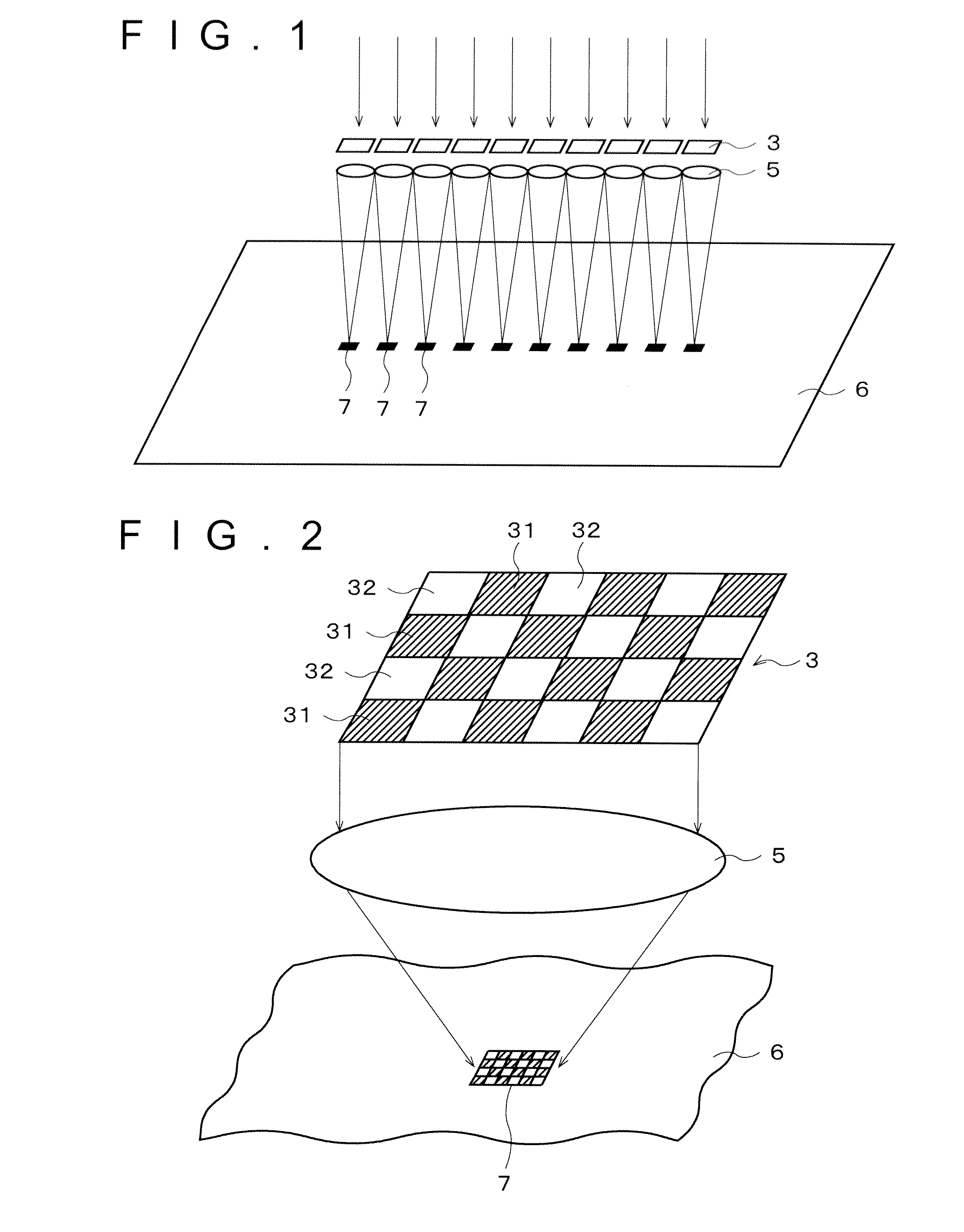
[0037]In Embodiment 1, the light-blocking areas 31 and transmission areas 32 of the mask 4 are not limited to being of rectangular shape; they can be circular or any of a variety of other shapes. Furthermore, the approach adopted in the embodiment described above was that no mask be used in step 2 besides the light-blocking areas for defining the channel areas, but it is possible to use a mask in step 2 as well, and make the parts used as light-blocking areas in step 1 into transmission areas, and the parts used as transmission areas in step 1 into light-blocking areas. The laser light is directed only on the parts of the a-Si:H film that remain amorphous in step 1, and these parts are annealed. Furthermore, in such an instance, it is permissible to make the transmission areas in step 2 smaller than the light-blocking areas of step 1, and provide a gap between the laser light irradiation areas in step 1 and the laser light irradiation areas in step 2. This will make it possible to p...

embodiment 2

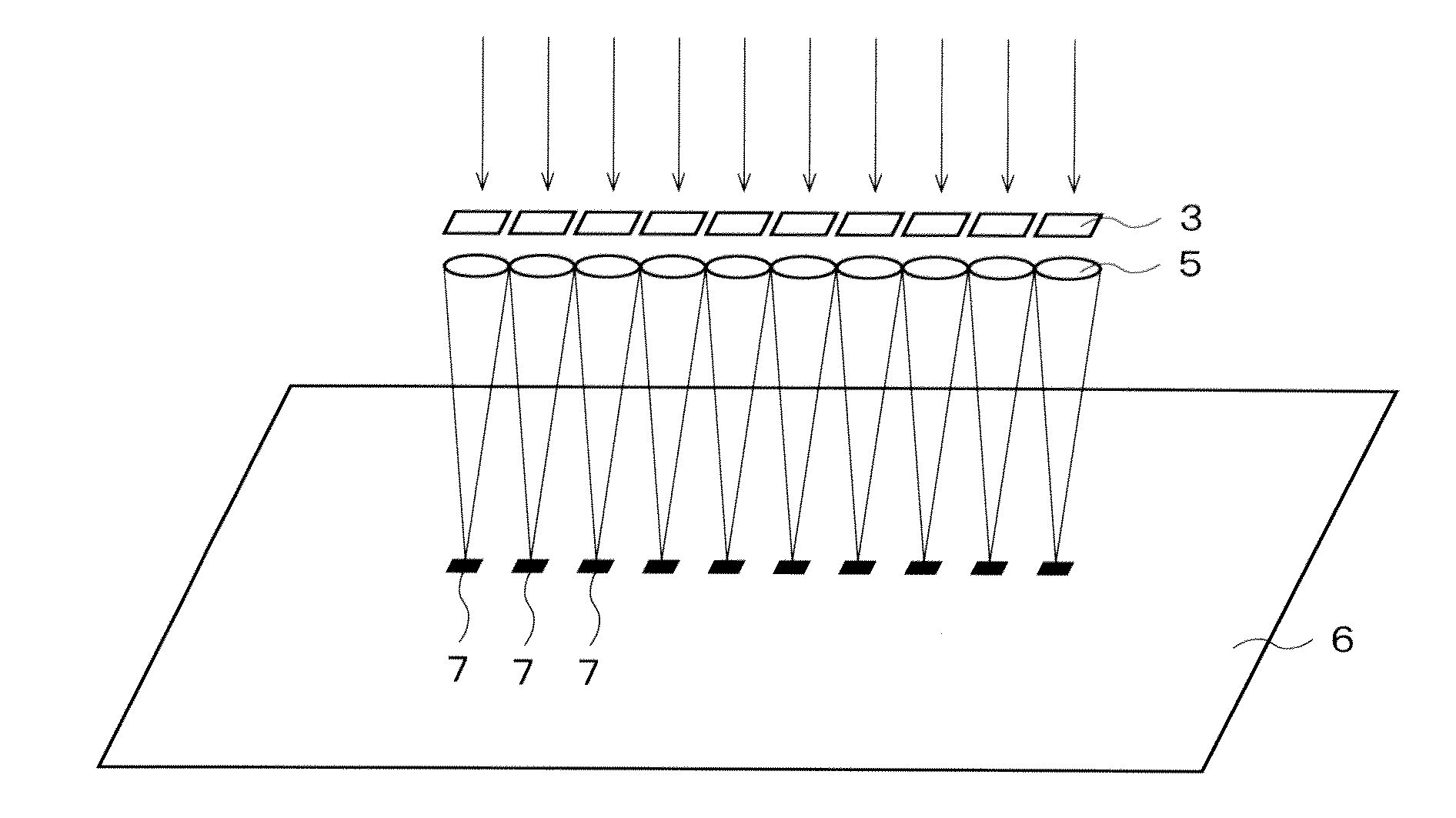
[0039]There shall now be described a method for forming a low-temperature polysilicon film using the forming device of Embodiment 2. First, in step 1, laser light is directed, using the microlenses 5, on the planned channel-area-formation areas 7 of the object of irradiation 6, using the mask 8. An irradiation pattern where areas irradiated by the laser light in a spot-shaped configuration are interspersed at equidistant intervals is obtained in the planned area 7. The areas where the laser light is directed in a spot-shaped configuration is where the a-Si:H film melts and solidifies to yield polycrystallized polysilicon.

[0040]Next, the mask 8 is removed and the entirety of the planned area 7 is irradiated with laser light. With the spot-shaped areas polycrystallized in step 1 serving as seeds, crystallization occurs and the entirety of the planned area 7 becomes a polysilicon film. In this case, the seeds for crystallization in the resulting polysilicon film are the already-polycry...

embodiment 3

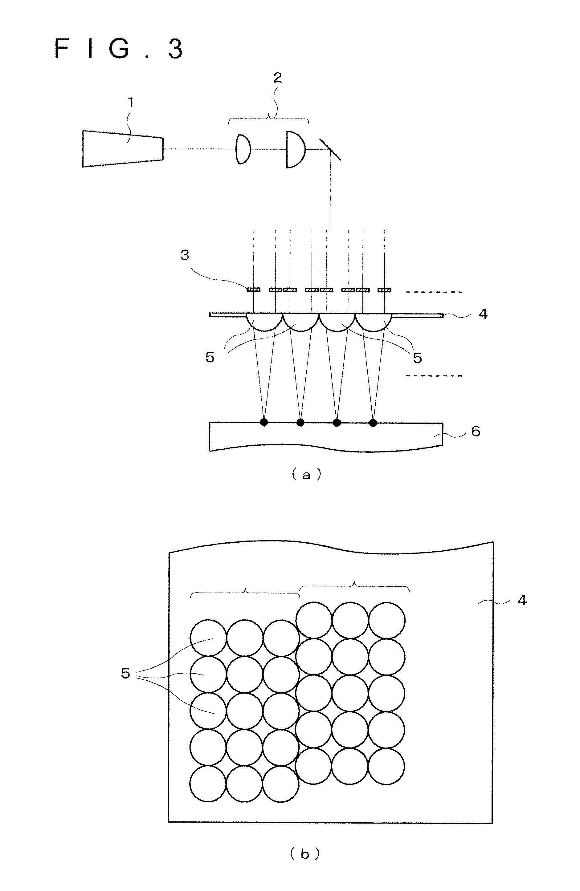
[0043 of the present invention will now be described with reference to FIG. 5. The mask 9 in FIG. 5 is configured by cutting out from a light-blocking member 91 a plurality of rectangular holes at a prescribed relative spacing, the light-blocking member 91 formed using a material that blocks laser light. A plurality of transmission areas 92 comprising the plurality of rectangular holes is arranged two-dimensionally. The transmission areas 92 are surrounded by light-blocking areas comprising the light-blocking member 91, and are partitioned by the light-blocking areas.

[0044]There shall now be described a method for forming a low-temperature polysilicon film using the forming device of Embodiment 3. First, in step 1, laser light is directed via the microlens 5 on the planned channel-area-formation area of the object of irradiation 6 using the mask 9. As with Embodiment 1, only the laser light that passes through the transmission areas 92 of the mask 9 is directed onto the amorphous si...


PUM

PropertyMeasurementUnit
softening pointaaaaaaaaaa
wavelengthaaaaaaaaaa

Abstract

Provided is a forming device and method making it possible to obtain a low-temperature polysilicon film in which the size of crystal grains fluctuates minimally, and is uniform. A mask has laser-light-blocking areas and laser-light-transmission areas arranged in the form of a grid such that the light-blocking areas and transmission areas are not adjacent to one another. Laser light is directed by the microlenses through the masks to planned channel-area-formation areas. The laser light transmitted by the transmission areas is directed onto an a-Si:H film, annealing and polycrystallzing the irradiated parts thereof. The mask is then removed, and when the entire planned channel-area-formation area is irradiated with laser light, the already-polycrystallized area, having a higher melting point, does not melt, while the area in an amorphous state melts and solidifies, leading to polycrystallization. The grain size of the polysilicon film obtained is regulated by the light-blocking areas and transmission areas and is thus controlled to a predetermined range.

Description

TECHNICAL FIELD[0001]The present invention relates to a device and method for forming a low-temperature polysilicon film in which an amorphous silicon film (“a-Si film”) is irradiated with and annealed by laser light, whereby the a-Si is crystallized to polycrystalline silicon (“polysilicon”).BACKGROUND ART[0002]An example of a thin film transistor of a reverse stagger construction is an amorphous silicon transistor. Such transistors are obtained by forming a gate electrode on an insulated substrate from a metallic layer made of Cr, Al, or the like; forming, e.g., a SiN film as a gate insulation film on the substrate including the gate electrode; subsequently forming a hydrogenated amorphous silicon (“a-Si:H”) film over the entire surface; patterning the a-Si:H film in island shapes in predetermined areas on the gate electrode; and forming source and drain electrodes from the metal layer.[0003]However, since such amorphous silicon transistors have an a-Si:H film in the channel area,...

Claims


Application Information

Patent Timeline
Patent Type & Authority Applications(United States)
IPC IPC(8): H01L21/268B23K26/06H01L21/336H01L29/786
CPCH01L21/02532H01L21/02595H01L21/0268H01L21/268G03F1/14C30B1/023C30B13/22C30B29/06H01L27/1285G03F1/62
Inventor KAJIYAMA, KOICHIHAMANO, KUNIYUKIMIZUMURA, MICHINOBU
Owner V TECH CO LTD
Why Eureka
Try Eureka