

Organic el device and method for manufacturing same
- Summary
- Abstract
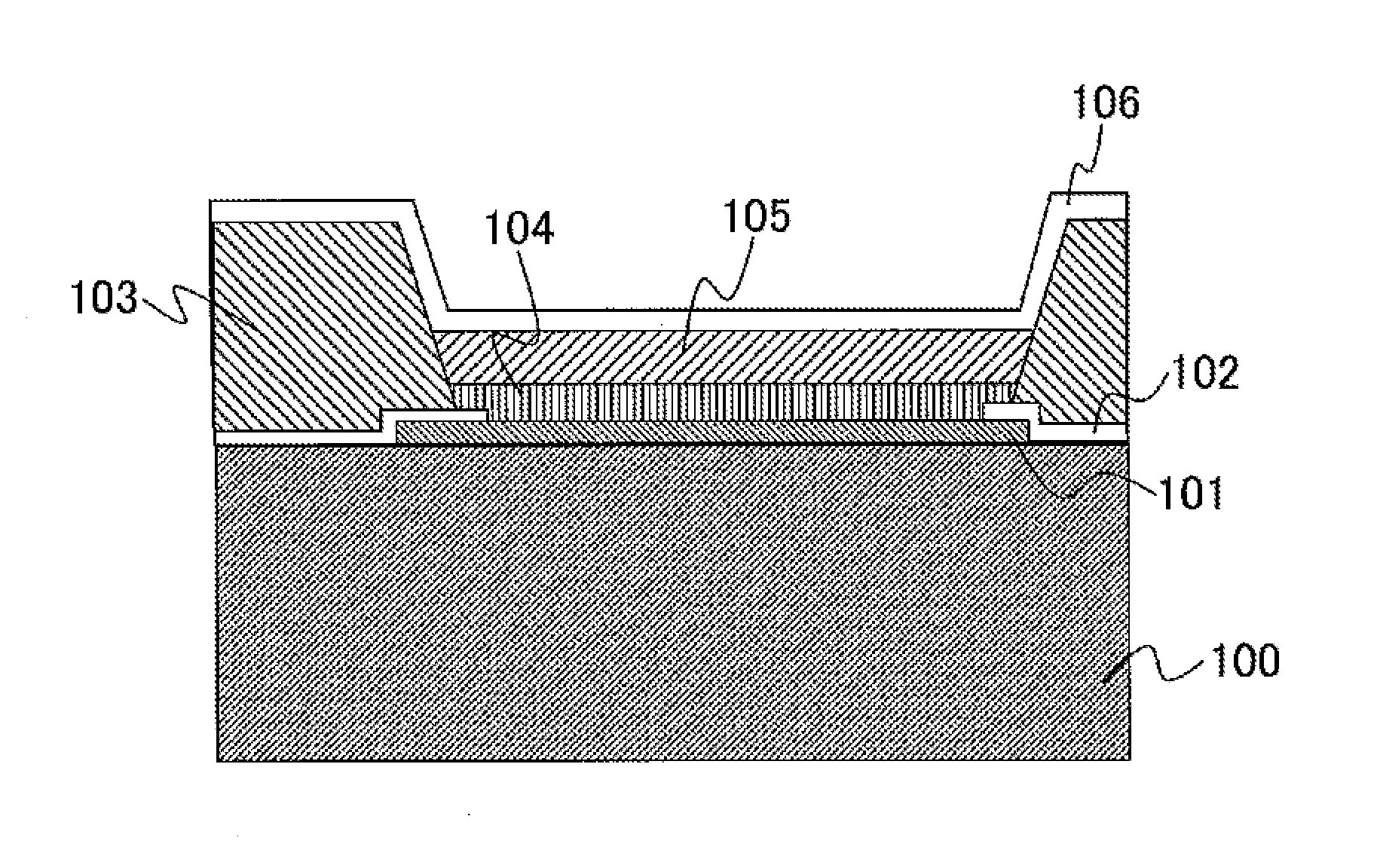
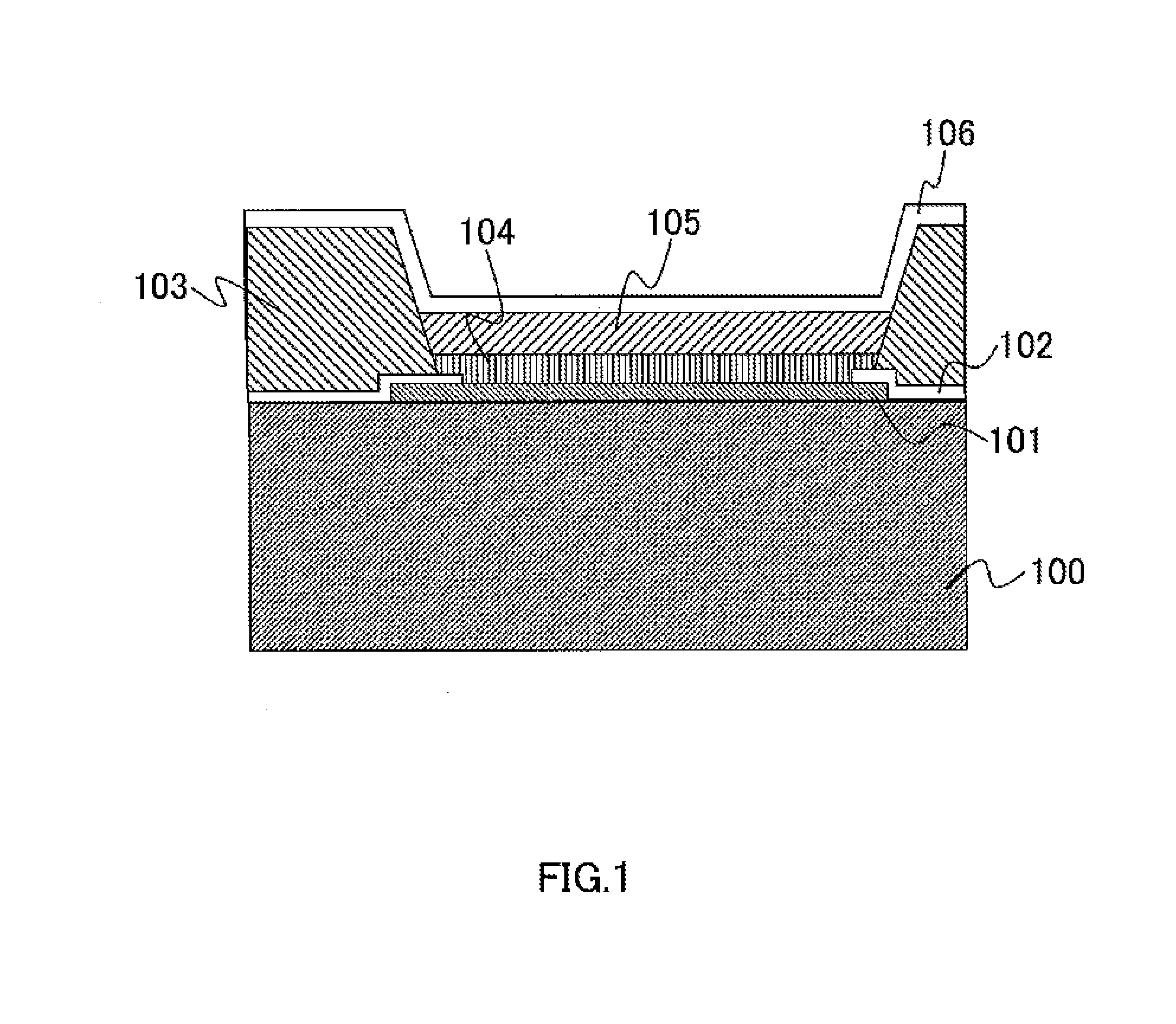
- Description
- Claims
- Application Information
AI Technical Summary
Benefits of technology
Problems solved by technology
Method used
Image

Examples
experimental example 1
[0168]Titanium oxide (TiOx) film having a thickness of 50 nm is formed by sputtering on a glass substrate measuring 100 mm per side (EAGLE 2000, Matsunami Glass Ind., Ltd.) as a model of the hole injection layer. The deposition condition is set as follows: the target is sintered TiO2, the Ar gas pressure is around 1 Pa, and RF output is 300W.
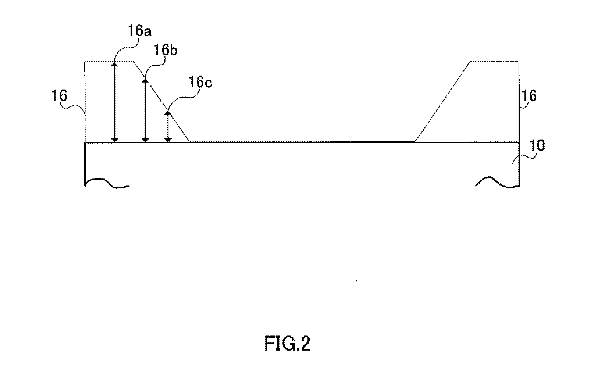
[0169]A bank is formed on the formed titanium oxide (TiOx) film by photolithography. An acrylic resin (Asahi Glass Co., Ltd.), the acrylic resin containing fluorine compounds, is used as a material of the bank. Further, as the material of the bank, a negative material, which undergoes cross-link reaction and is cured when being exposed with a light, is used. The bank is patterned a film formed by spin coating by pre-baking a film formed by spin coating at the temperature of 100° C. for two minutes; irradiating the film with ultraviolet light via a photomask; and developing the film using 0.2% of a Tetra Methyl Ammonium Hydroxide (TMAH) aqueous s...
PUM
 Abstract
Description
Claims
Application Information