

Semiconductor device
- Summary
- Abstract
- Description
- Claims
- Application Information
AI Technical Summary
Benefits of technology
Problems solved by technology
Method used
Image

Examples
embodiment 1
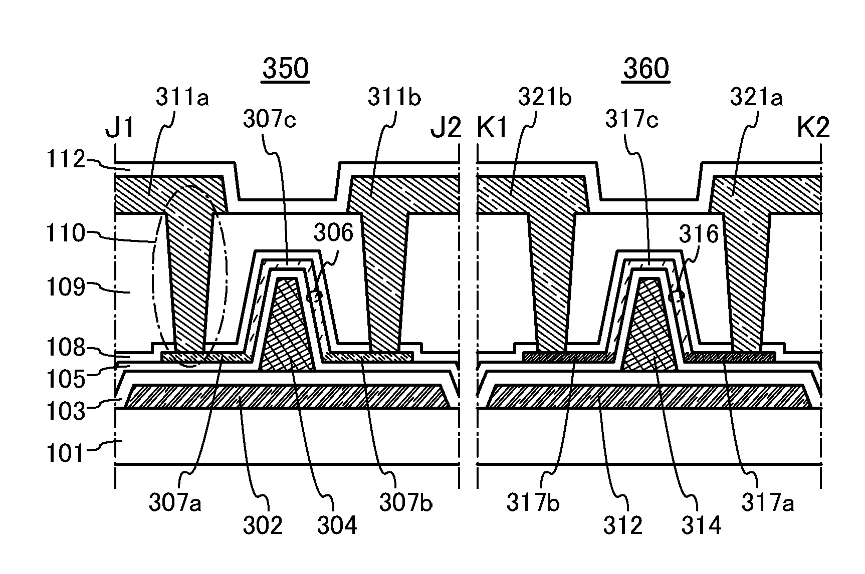
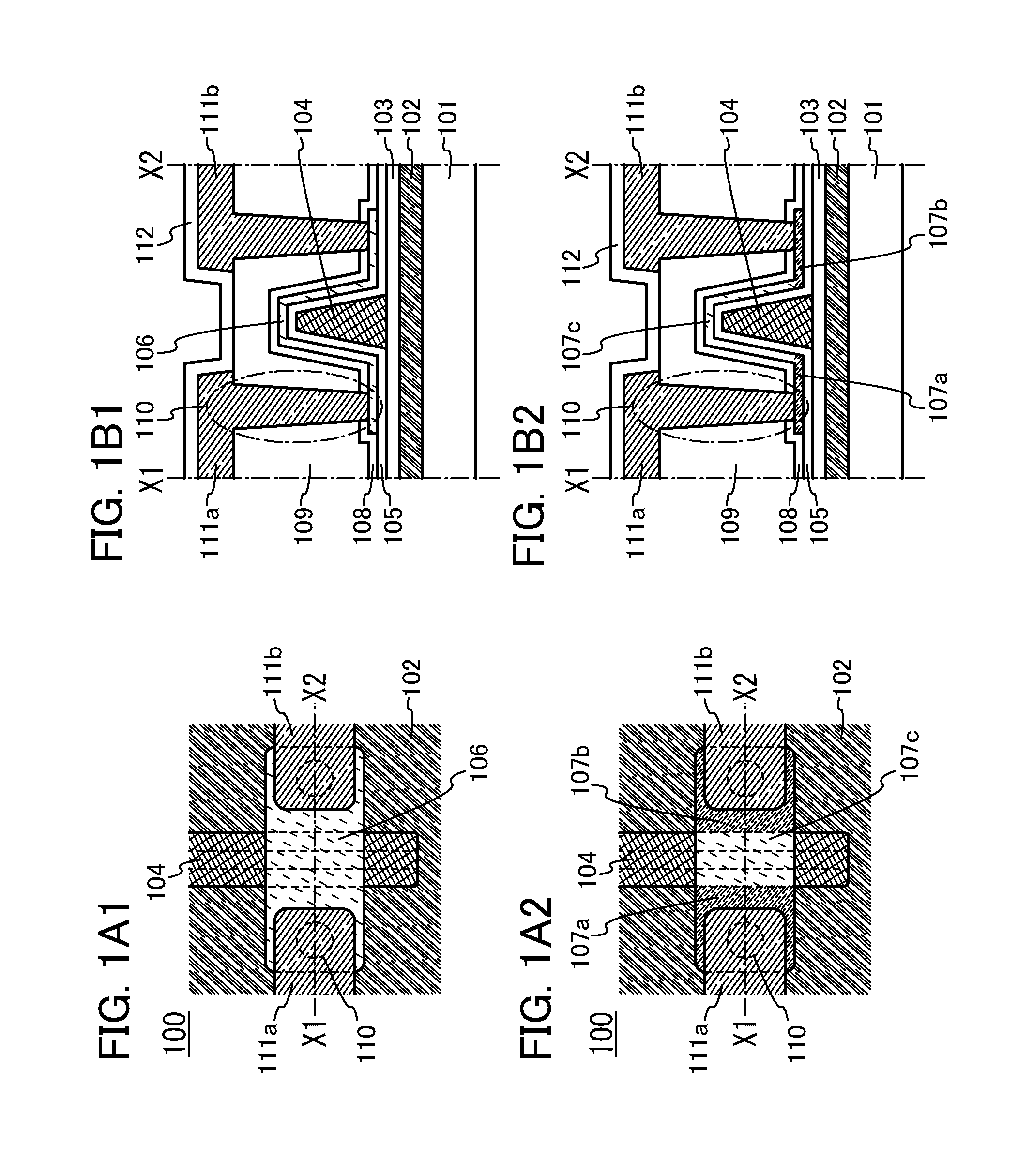
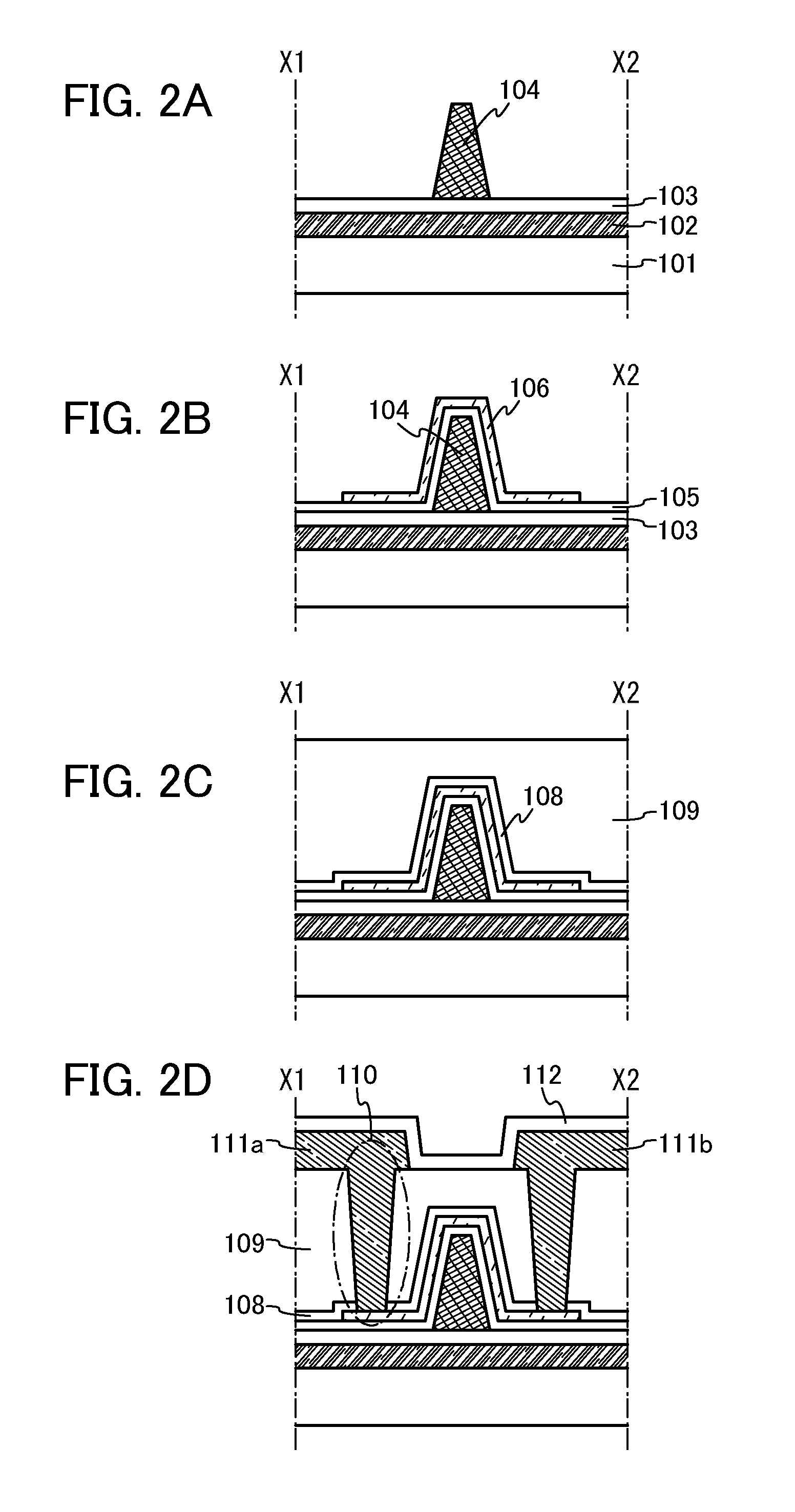
[0057]This embodiment describes a structure of a transistor and a method for manufacturing the transistor, each of which is one embodiment of the present invention, with reference to FIGS. 1A1, 1A2, 1B1, and 1B2, FIGS. 2A to 2D, and FIGS. 3A to 3C.
[0058]FIG. 1A1 is a top view of a transistor 100. FIG. 1B1 is a cross-sectional view taken along X1-X2 in FIG. 1A1. FIG. 1A2 is a top view of the transistor 100. FIG. 1B2 is a cross-sectional view taken along X1-X2 in FIG. 1A2. Note that FIGS. 1B1 and 1B2 are cross-sectional views of the transistor 100 in the channel length direction.
[0059]In the transistor 100, an electrode 102 is formed over a substrate 101. An insulating layer 103 is formed over the electrode 102, and a gate electrode 104 is formed over the insulating layer 103. The gate electrode 104 has a height (thickness) larger than the length of the lower base in the cross section in the channel direction.
[0060]A gate insulating layer 105 is formed over the gate electrode 104. A s...
embodiment 2
)
[0147]This embodiment describes a transistor 150 which is partly different from the transistor 100 described in Embodiment 1 with reference to FIGS. 4A to 4C.
[0148]FIG. 4A is a top view of the transistor 150. FIGS. 4B and 4C are cross-sectional views taken along Y1-Y2 in FIG. 4A. Note that FIGS. 4B and 4C are cross-sectional views of the transistor 150 in the channel length direction.
[0149]The transistor 150 described in this embodiment differs from the transistor 100 described in Embodiment 1 in the structure of the gate insulating layer. To miniaturize semiconductor elements, thinning of a gate insulating layer is required in accordance with the scaling law. In thinning of a gate insulating layer, an increase in leakage current and a decrease in withstand voltage due to defects such as pin holes become problems. Considering the above fact, a gate insulating layer of the transistor 150 is formed by an anodic oxidation method.
[0150]FIG. 4B illustrates a cross-sectional structure of...
embodiment 3
[0159]This embodiment describes a structure example of a memory device as an example of a semiconductor device including the transistor disclosed in this specification, with reference to FIGS. 5A to 5D and FIG. 6.
[0160]FIG. 5A is a top view of a memory cell 210 in a memory device. FIG. 5B is a cross-sectional view taken along Z1-Z2 in FIG. 5A. FIG. 5C is an equivalent circuit diagram of the memory cell 210. FIG. 5D is a conceptual view of a memory device including the memory cells 210. The memory cell 210 in this embodiment has a structure corresponding to a so-called DRAM (dynamic random access memory).
[0161]The memory cell 210 includes a transistor 201 and a capacitor 202. The transistor described in any of the above embodiments can be used as the transistor 201. The source and drain regions 107a and 107b in the transistor 201 are formed by supply of a potential to the electrode 102. The capacitor 202 is formed from the drain region 107b and the electrode 102 serving as electrodes...
PUM
 Abstract
Description
Claims
Application Information