Chip-last embedded interconnect structures and methods of making the same

a technology of embedded interconnects and chiplasts, applied in the direction of printed circuit non-printed electric components, immunological disorders, metabolism disorders, etc., can solve the problems of complex fabrication of multiple substrate layers and cavity formation of chips, and the associated cost of the substrate can be relatively high

Inactive Publication Date: 2012-09-13
GEORGIA TECH RES CORP
View PDF9 Cites 56 Cited by
  • Summary
  • Abstract
  • Description
  • Claims
  • Application Information

AI Technical Summary

Problems solved by technology

Alternative technology, called “chip-last” technology has the potential to overcome manufacturing and business challenges of chip-first technology, however chip-last technology also presents challenges.
For example, the fabrication of multiple substrate layers and cavity formation for the chip can be difficult, and the associated cost of the substrate can be relatively high, and thus undesirable.

Method used


Image

  • Chip-last embedded interconnect structures and methods of making the same
  • Chip-last embedded interconnect structures and methods of making the same
  • Chip-last embedded interconnect structures and methods of making the same

Examples


example 1

Chip-Last Embedding in 1-2 Metal Layer Structure

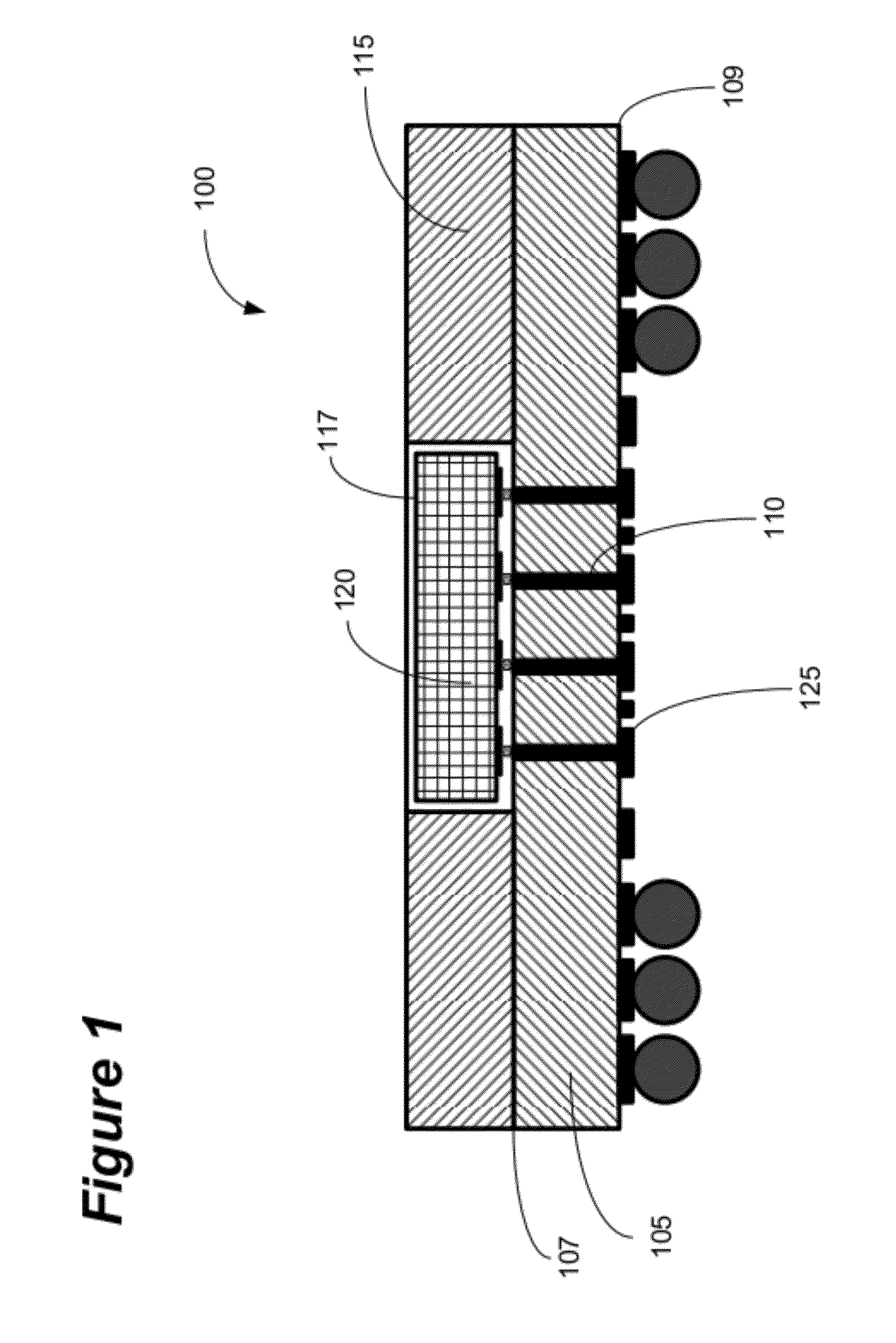
[0060]To achieve embedding of a 70-100 μm pitch area array I / O IC in core, an innovative two-metal layer substrate with ultra-high wiring density has been developed. The substrate structure is obtained by a two-step process—(1) fabrication of the thin core substrate with fine-pitch through-holes and fine line width and spaces, and (2) lamination of another thin-core substrate with pre-formed cavity for die embedding. This innovative approach has two major novelties—(1) ultra-fine metal lines and spaces on core laminate and (2) ultra-fine pitch through-holes. Instead of conventional wet etching process, the semi-additive process (SAP), usually used for build-up layer to achieve 10 μm and sub-10 μm lines and spaces was employed for fabrication of ultra-fine copper traces on the core. UV laser with 266 nanometers (nm) wavelength was employed for ultra-fine pitch (70-100 μm) through-holes to meet the fine-pitch flip-chip I / O needs.

TABLE 1P...

example 2

Fine Lines / Spaces on Core

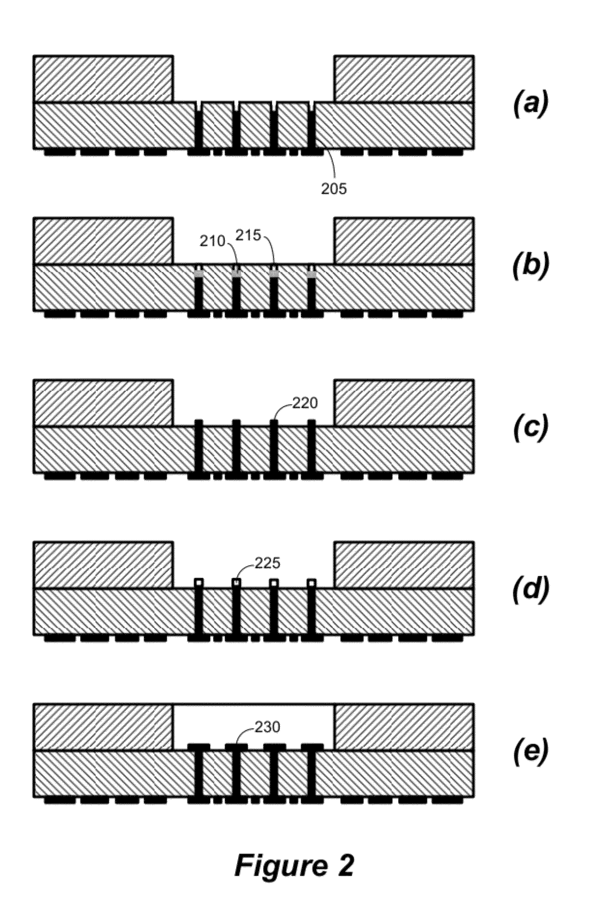
[0062]To fabricate 7-15 μm line widths and spaces for copper circuitry on core laminate, the SAP method was employed instead of the conventional wet etching method. The first step is surface copper removal from a double sided copper clad laminate. Following copper removal, surface desmear and electroless copper plating was done to form a thin copper seed layer on the surface. Thereafter, a layer of dry film photo resist was laminated, exposed, and developed. Once the circuitry pattern was transferred to the photo resist, the electrolytic copper plating was carried out to plate the pattern in the photo-resist mold. After photo resist stripping, the final step is to remove the seed copper layer by micro etching. The process flow is described in FIG. 13.

[0063]The process mentioned above enables the wiring density of the 1+2+1 substrate within a two metal layer thin core with filled through holes and ultra fine lines. The reduction in layer count by elimination ...

example 3

Ultra-fine Pitch Area-Array Through-holes

[0064]The biggest challenge in achieving a substrate structure is fabrication of small diameter through-holes at ultra-fine pitch to meet the chip I / O footprint such that no escape routing is needed on the chip attach side of the module. The concern with ultra-fine pitch area array through-hole fabrication is the wall-to-wall distance of adjacent holes. If the wall-to-wall distance is not large enough, there is a high probability of encountering mechanical strength related issues. Therefore, in order to make ultra-fine pitch area-array through-holes, it is important to fabricate the holes with small diameter.

[0065]Currently, two techniques are most commonly used to make through-holes on glass-fiber reinforced laminates—(1) mechanical drilling, and (2) laser drilling. The most established through-hole technology is mechanical drilling. Mechanical drilling is an effective method for through-hole diameters larger than 150 μm. Current the-state-o...


PUM


Abstract

The various embodiments of the present invention provide a novel chip-last embedded structure, wherein an IC is embedded within a one to two metal layer substrate. The various embodiments of the present invention are comparable to other two-dimensional and three-dimensional WLFO packages of the prior art as the embodiments have similar package thicknesses and X-Y form factors, short interconnect lengths, fine-pitch interconnects to chip I / Os, a reduced layer count for re-distribution of chip I / O pads to ball grid arrays (BGA) or land grid arrays (LGA), and improved thermal management options.

Description

CROSS-REFERENCE TO RELATED APPLICATION[0001]This application claims the benefit of U.S. Provisional Patent Application Ser. No. 61 / 450,432, filed 8 Mar. 2011, which is incorporated herein by reference in its entirety as if fully set forth below.BACKGROUND[0002]1. Field[0003]The various embodiments of the present invention relate to chip-last embedded interconnect structures and methods of making the same.[0004]2. Description of Related Art[0005]The trend in miniaturized and highly-functional electronic modules is driving the need for embedded actives and passives that enables highly-complex heterogeneous sub-systems and systems. Two-types of embedding technologies currently exists, both of which are based on “chip-first” techniques and include (1) embedding by wafer-level fan-out (WLFO), and (2) embedding in organic substrates. Alternative technology, called “chip-last” technology has the potential to overcome manufacturing and business challenges of chip-first technology, however c...

Claims


Application Information

Patent Timeline
Patent Type & Authority Applications(United States)
IPC IPC(8): H01L25/07H01L23/495
CPCH01L23/13H01L2924/15153H01L23/49833H01L25/105H01L2224/16225H01L25/0657H01L2224/16227H01L2225/06517H01L2225/1058H01L2924/15311H01L2225/06572H01L25/16H01L2225/1029H01L2225/1052H01L2224/73253H01L23/49827H01L2224/05573H01L2224/05568H01L2924/00014A61P11/06A61P19/00A61P25/00A61P25/28A61P29/00A61P3/00A61P35/00A61P37/00A61P37/08A61P5/00A61P9/00H01L2924/15321H01L2924/15192H01L2224/16235H01L2224/05599
Inventor LIU, FUHANSUNDARAM, VENKATESHKUMBHAT, NITESHTUMMALA, RAO
Owner GEORGIA TECH RES CORP
Why Eureka
Try Eureka