Semiconductor device and method for manufacturing the same

a semiconductor layer and semiconductor technology, applied in the field of semiconductor devices, can solve the problems of difficult to greatly increase the thickness of the semiconductor layer of the tfd, rate-limiting factor, and inability to achieve high sensitivity, so as to ensure the sensing sensitivity to visible light, increase the sensing sensitivity to infrared rays, and easy production

Inactive Publication Date: 2012-09-27
SHARP KK
View PDF51 Cites 18 Cited by
  • Summary
  • Abstract
  • Description
  • Claims
  • Application Information

AI Technical Summary

Benefits of technology

[0025]According to the present invention, in a semiconductor device provided with a first and a second thin film diodes in which wavelength regions of light to be detected are mutually different on one and the same substrate, light in the wavelength region to be detected by respective one of the thin film diodes can be efficiently incident on the semiconductor layer of the corresponding thin film diode. As a result, both of the effective sensitivities of a sensor utilizing the first thin film diode and a sensor utilizing the second thin film diode can be obtained sufficiently.
[0026]Particularly, the present invention is preferably applied to a semiconductor device provided with a d

Problems solved by technology

In this case, since a semiconductor layer (the low-temperature poly-silicon layer) of the TFD is thin, the semiconductor layer of the TFD cannot sufficiently absorb light having relatively longer wavelength (e.g. red light) and there is some possibility that high sensitivity cannot be attained.
However, if the semiconductor layer is made thicker, the process for crystallizing an amorphous silicon film by

Method used


Image

  • Semiconductor device and method for manufacturing the same
  • Semiconductor device and method for manufacturing the same
  • Semiconductor device and method for manufacturing the same

Examples


first embodiment

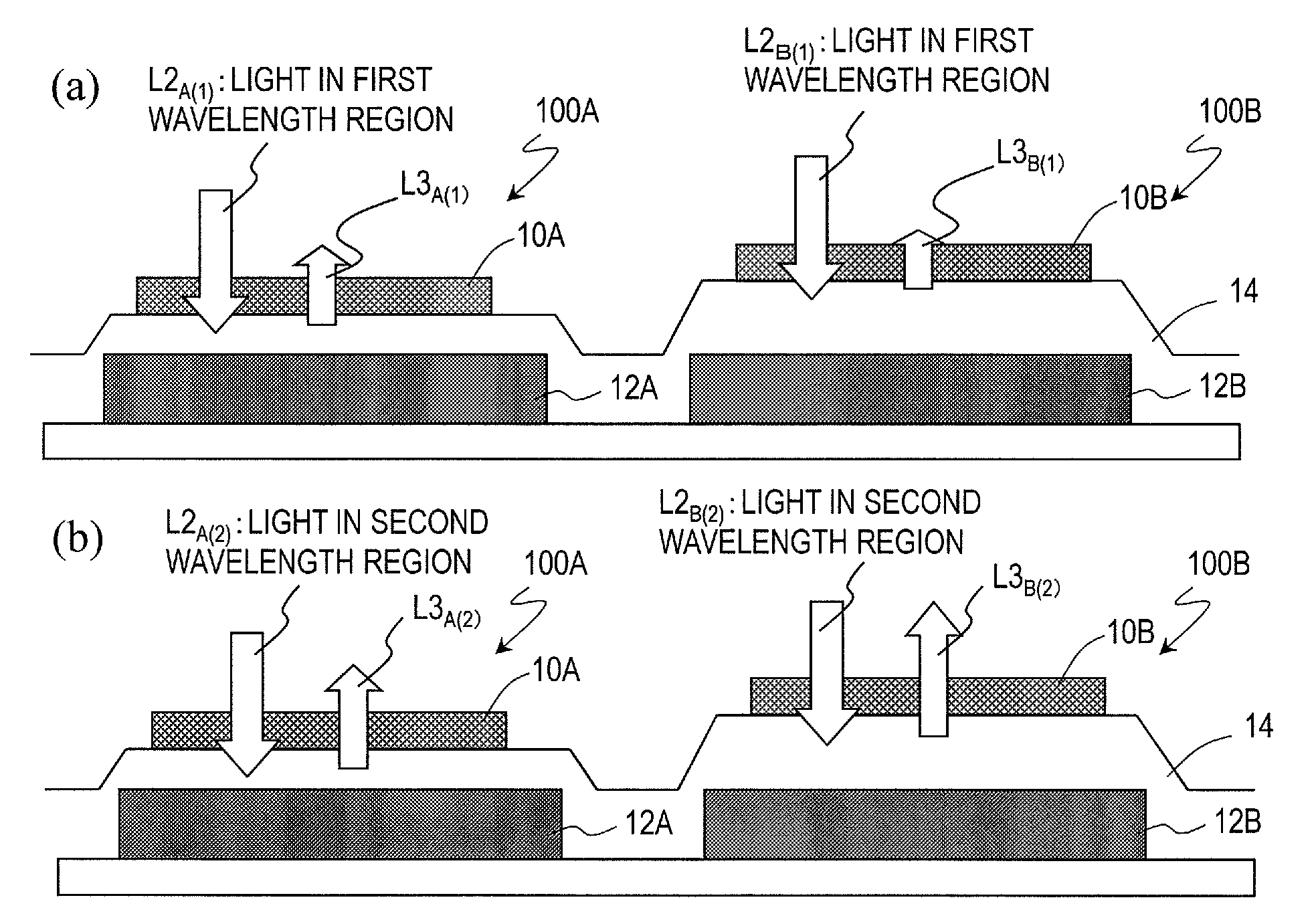
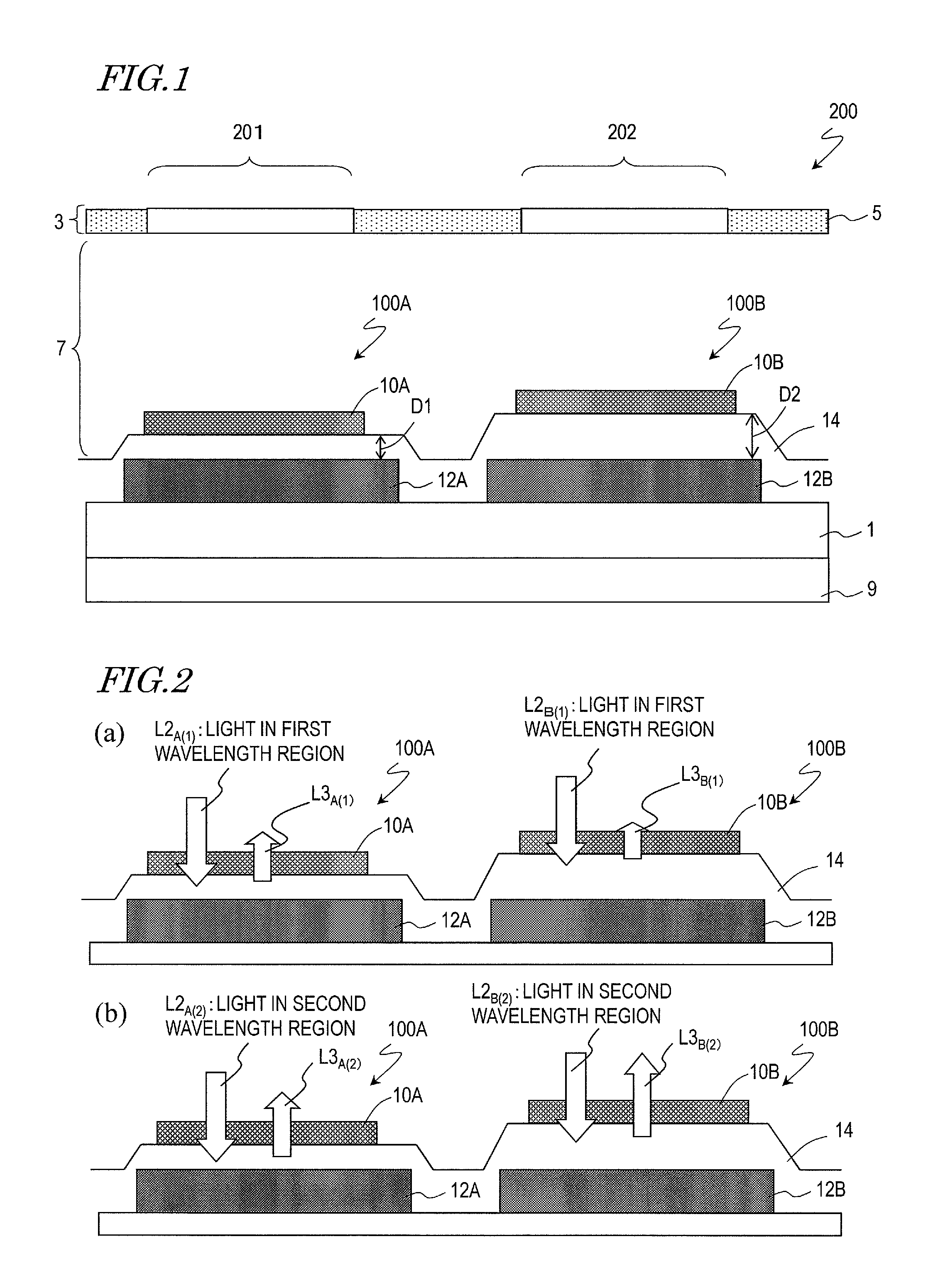
[0056]Hereinafter, a first embodiment of a semiconductor device of the present invention will be described. The semiconductor device in the present embodiment is a liquid crystal display device having an optical sensor portion utilizing a thin film diode, for example.

[0057]FIG. 1 is a schematic sectional diagram showing two thin film diodes 100A and 100B in the semiconductor device in the present embodiment. For simplicity, the components similar to those in FIG. 11 are designated by the same reference numerals, and the descriptions thereof are omitted.

[0058]A semiconductor device 200 in the present embodiment is provided with an optical sensor portion including a first sensor 201 for detecting light in a first wavelength region and a second sensor 202 for detecting light in a second wavelength region. The first sensor 201 has a first thin film diode 100A, and the second sensor 202 has a second thin film diode 100B, respectively. The second wavelength region includes a wavelength lo...

second embodiment

[0101]Hereinafter with reference to the drawings, a second embodiment of the semiconductor device of the present invention will be described. The semiconductor device in the second embodiment is different from the first embodiment in that in addition to the two types of thin film diodes, a thin film transistor is formed on one and the same substrate. The present embodiment can be applied to an active matrix display device having an optical sensor portion such as a touch sensor, a scanner, or the like. The two types of thin film diodes may be connected in parallel, so as to constitute an optical sensor portion. The thin film transistor may be a pixel switching TFT disposed for each pixel in a display area of a display device, or may be a TFT for a circuit which constitutes a driving circuit in an area other than the display area (in a frame area). Alternatively, the thin film transistor may be a signal taking-out TFT used in the optical sensor portion.

[0102]FIG. 6 is a schematic sect...

third embodiment

[0118]In the present embodiment, a display device provided with a sensor function. The display device is configured by using a semiconductor device of any one of the above-described embodiments.

[0119]The display device provided with the sensor function in the present embodiment is, for example, a liquid crystal display device with a touch sensor which includes a display area and a frame area located around the display area. The display area has a plurality of display portions (pixels) and a plurality of optical sensor portions. Each display portion includes a pixel electrode and a pixel switching TFT, and each optical sensor portion includes two types of optical sensors for mutually different wavelength regions to be detected. Each optical sensor includes a TFD. In the frame area, a driving circuit for display is provided so as to drive each display portion, and a TFT for a driving circuit is utilized for the driving circuit. The pixel switching TFT and the TFT for a driving circuit...


PUM


Abstract

A first thin film diode (100A) has a first semiconductor layer (10A) and a first light blocking layer (12A) disposed on the substrate side of the first semiconductor layer. A second thin film diode (100B) has a second semiconductor layer (10B) and a second light blocking layer (12B) disposed on the substrate side of the second semiconductor layer. An insulating film (14) is formed between the first semiconductor layer (10A) and the first light blocking layer (12A) and between the second semiconductor layer (10B) and the second light blocking layer (12B). A thickness D1 of a portion of the insulating film (14) positioned between the first semiconductor layer (10A) and the first light blocking layer (12A) is different from a thickness D2 of a portion of the insulating film (14) positioned between the second semiconductor layer (10B) and the second light blocking layer (12B). The intensity of light in a first wavelength region incident on the first semiconductor layer (10A) is higher than the intensity of light in the first wavelength region incident on the second semiconductor layer (10B). The intensity of light in a second wavelength region including a wavelength longer than the maximum wavelength of the first wavelength region incident on the second semiconductor layer (10B) is higher than the intensity of light in the second wavelength region incident on the first semiconductor layer (10A).

Description

TECHNICAL FIELD[0001]The present invention relates to a semiconductor device including a thin film diode (Thin Film Diode: TFD), and a production method thereof.BACKGROUND ART[0002]In recent years, electronic equipment such as a display device or an image sensor provided with an optical sensor portion utilizing a TFD has been developed.[0003]Patent Document 1 discloses an image sensor in which an optical sensor portion utilizing a TFD and a driving circuit utilizing a thin film transistor (Thin Film Transistor: TFT) are provided on one and the same substrate. Patent Document 2 discloses a display device provided with an optical touch panel. In this display device, an optical sensor portion utilizing a TFD is provided in a display area of a liquid crystal display device, so that an object such as a finger which touches the screen can be detected by utilizing ambient light. In addition, Patent Document 3 discloses a display device provided with an optical touch panel in which an objec...

Claims


Application Information

Patent Timeline
IPC IPC(8): H01L31/113H01L31/18
CPCG02F1/1368G06F3/0412H01L29/78633H01L27/14623H01L27/14645H01L27/14621G06F3/042H01L27/14678
Inventor AICHI, HIROSHI
Owner SHARP KK
Why Eureka
Try Eureka