

Mold structures, and method of transfer of fine structures
a technology of fine structures and molds, applied in the field of nanoprint transfer methods, can solve the problems of difficulty in releasing molds from substrates, mold damage upon their release, and the problem of mold damage upon release has not yet been solved, and achieves the effect of high accuracy
- Summary
- Abstract
- Description
- Claims
- Application Information
AI Technical Summary
Benefits of technology
Problems solved by technology
Method used
Image

Examples
example 1
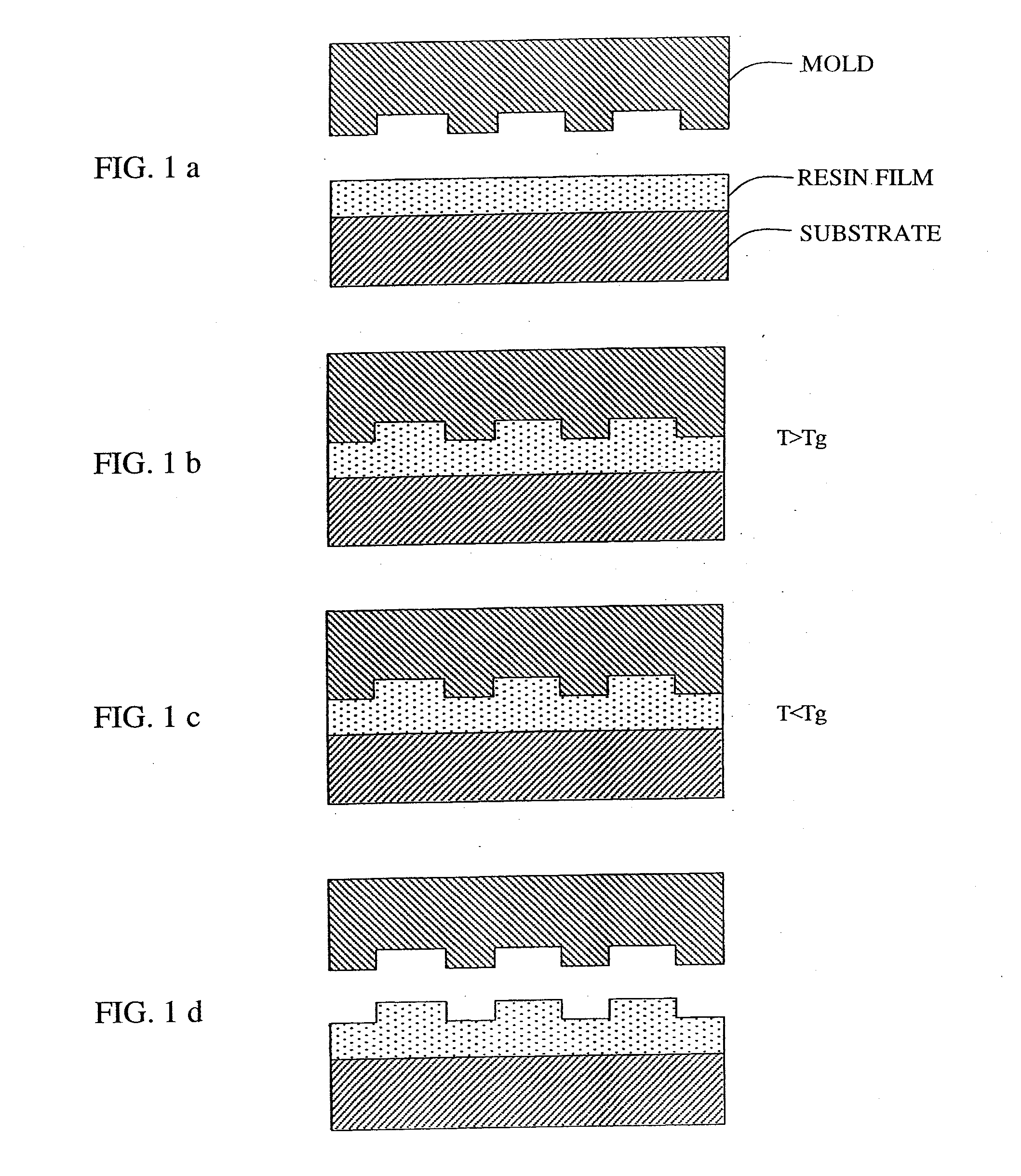
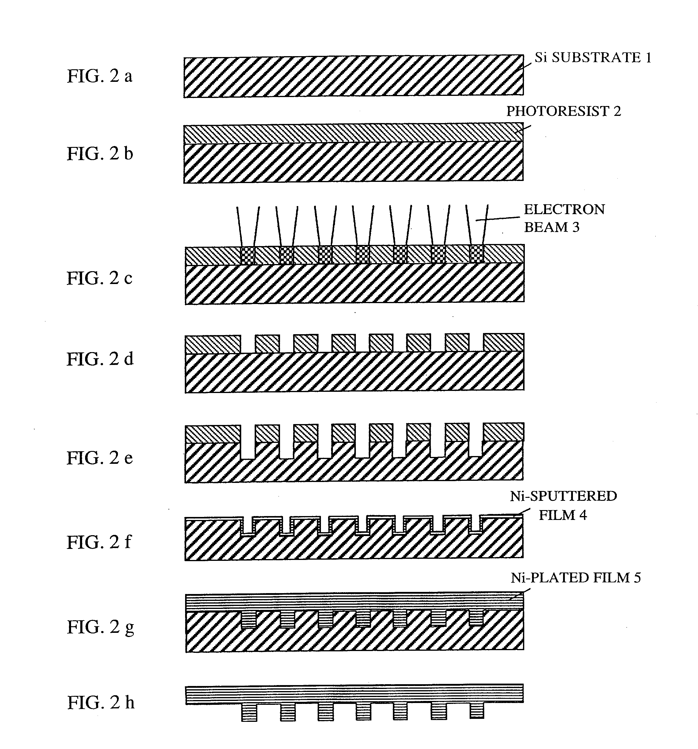
[0055]Referring to FIGS. 2 and 3, the method of producing a mold according to an embodiment of the invention will be described, which is flexible and fixed to a support frame via an elastomer. It should be noted that FIGS. 2 and 3 are conceptual diagrams in which pattern shapes are simplified and enlarged. Initially, an Si substrate 1 measuring 100 mm in length×100 mm in width×0.5 mm in thickness was prepared, as shown in FIG. 2(a). Then, a photoresist 2 (OEBR1000, manufactured by Tokyo Ohka Kogyo Co., Ltd.) for electron beam exposure was applied, using a spin coater, as shown in FIG. 2(b). Thereafter, using a JBX6000FS electron beam lithography apparatus (manufactured by Nippon Denshi), a pattern was directly drawn on the photoresist by an electron beam 3, as shown in FIG. 2(c), thus exposing the resist. The photoresist was then developed to obtain convex and concave portions formed on the substrate, as shown in FIG. 2(d). The remaining resist had circular patterns, each with a dia...
example 2
[0058]Referring to FIGS. 5 to 7, a method of producing a curved mold according to another embodiment of the invention will be described.
[0059]The Ni mold (6 inches, 100 μm in thickness) produced by the above-described process was bonded to an SUS (6 inches, with a thickness of 1 cm at the center and 7 mm at the edges) using a silicone adhesive (KE1820, manufactured by Shin-Etsu Silicones), and a pressure was exerted thereon (FIG. 5(a)), thereby obtaining a convex mold (FIG. 5(b)). It is possible to form a concave mold in a similar manner (FIG. 6).
[0060]Alternatively, it is possible to make a curved mold by performing Au 20-nm sputtering on a concave mold, conducting Ni electroplating until the center portion has a thickness of approximately 1 cm, and then releasing the deposited mold from the concave mold. Further, it is also possible to produce a concave mold by providing Ni plating on a convex mold in a similar manner.
[0061]Hereafter, the stamping process using a convex mold will ...
example 3
[0062]A method of producing a mold with a curved surface in which a deep groove is formed according to another embodiment of the invention will be described by referring to FIGS. 8 to 10.
[0063]A cross-shaped pattern with a width of 10 μm and a depth of 3 μm was formed in advance at the center of a Ni mold (6 inches, 100 μm in thickness). The mold was then bonded to an SUS (6 inches, with a thickness of 1 cm at the center and 7 mm at the edges), with a silicone adhesive (KE1820, manufactured by Shin-Etsu Silicones), thereby obtaining a deep-grooved convex mold (FIG. 8).
[0064]A stamping process was carried out using the above-described convex-curved mold with the deep groove. A 10% diethylene glycol monoethyl ether acetate solution of polystyrene 679 (manufactured by A & M Styrene Co., Ltd.) was applied to a 5-inch Φ Si substrate with a thickness of 0.5 mm, to a thickness of 500 nm. A 4-inch Φ buffer material of a thickness of 3 mm was then placed underneath. The base of the press mac...
PUM
 Abstract
Description
Claims
Application Information