Tunneling current amplification transistor

a technology of tunneling current and transistor, which is applied in the direction of transistors, semiconductor devices, electrical equipment, etc., can solve the problems of increasing static power consumption, unable to meet the requirements of low power consumption design in the future, and the theoretical limit of a conventional mosfet subthreshold slope of 60 mv/dec, etc., to increase the driving capability of the device and increase the on-current of the device

Inactive Publication Date: 2012-10-25
PEKING UNIV
View PDF3 Cites 4 Cited by
  • Summary
  • Abstract
  • Description
  • Claims
  • Application Information

AI Technical Summary

Benefits of technology

[0010]As compared with the conventional TFET, the tunneling current amplification transistor of the present ...

Problems solved by technology

The theoretical limit of a subthreshold slope of a conventional MOSFET is 60 mV/dec due to the limitation of thermoelectric force.
As the device size decreases, the threshold voltage of the device decreases and a static leakage current of the device deteriorates inevitably, leading to an increase of the static power consumption and thus the requirement of low power consumption design in the future can...

Method used


Image

  • Tunneling current amplification transistor
  • Tunneling current amplification transistor
  • Tunneling current amplification transistor

Examples


Embodiment Construction

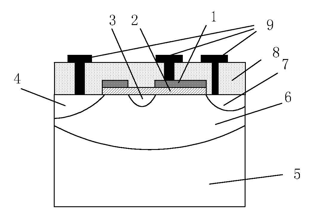
[0020]The implementation of a tunneling current amplification transistor of the invention will be further described below by specific embodiments and in combination with the accompany drawings.

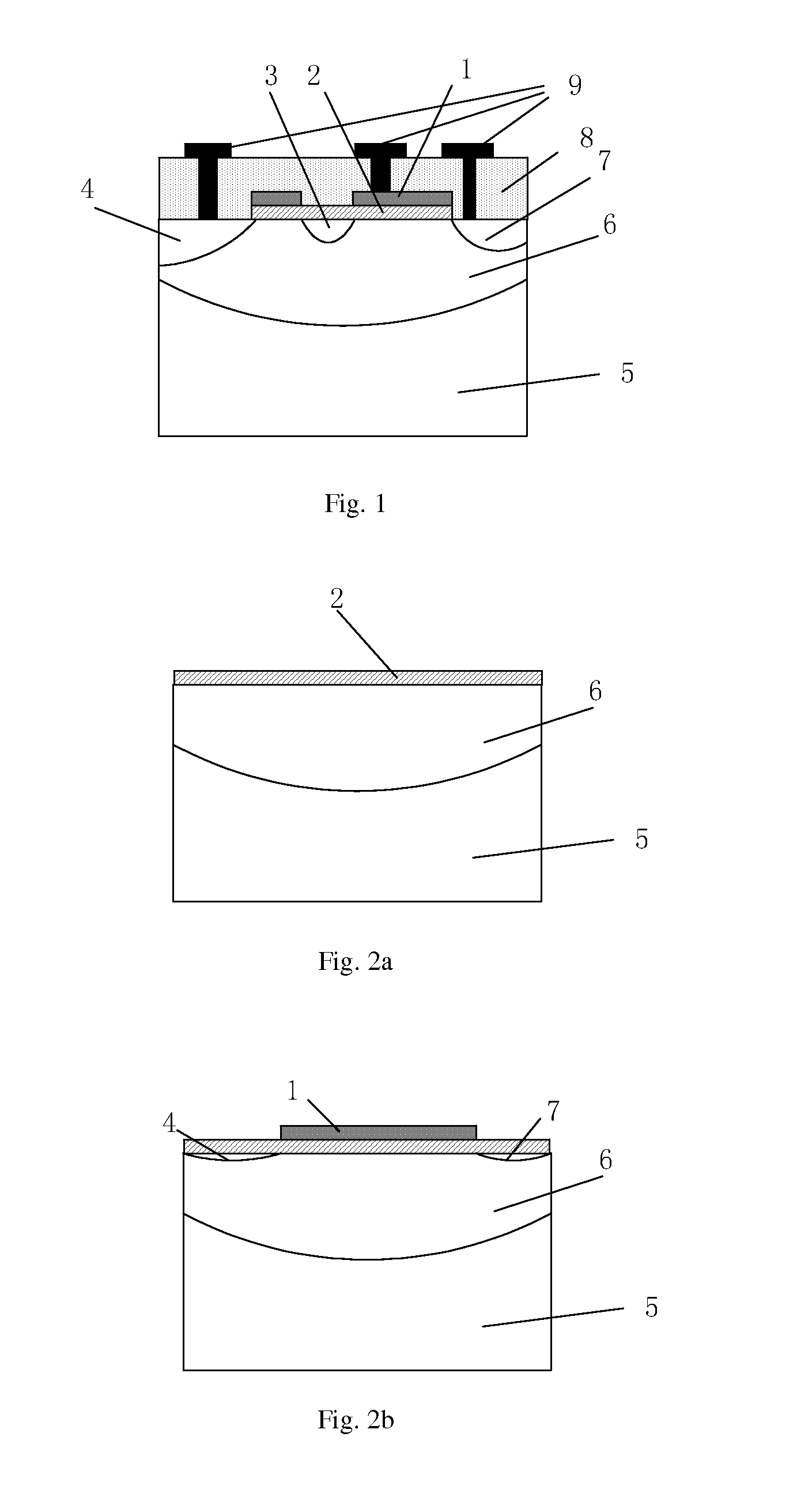
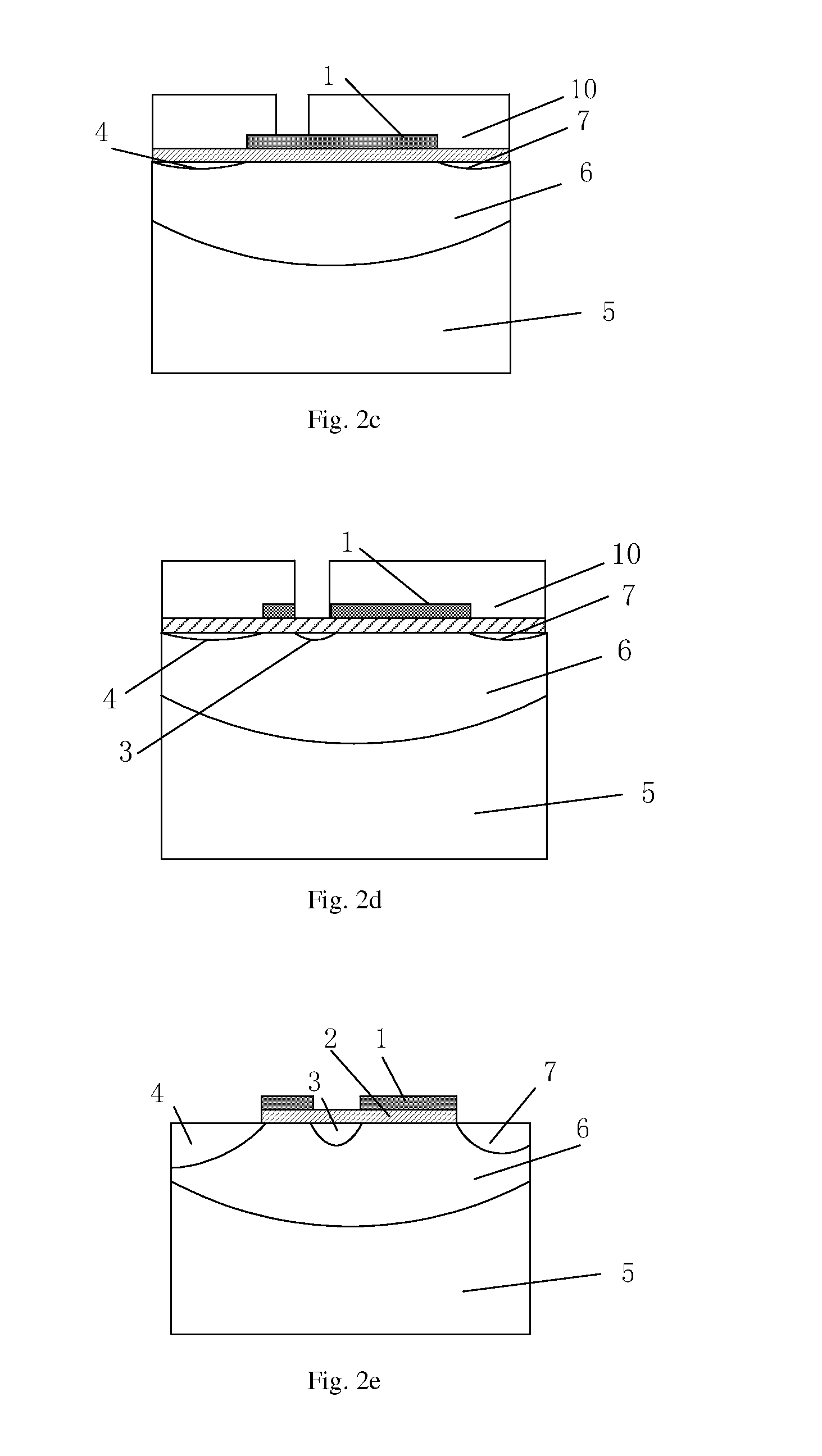
[0021]The specific implementation steps are as shown in FIGS. 2a-2f.

[0022]1. A gate oxide layer (i.e., a gate dielectric layer) 2 is growed on a semiconductor substrate 5. A silicon nitride is deposited, and a photolithography is performed on the active region. Then, a well implantation is performed and subsequently a well thermal diffusion is performed to form a well 6, as shown in FIG. 2a (the purpose of forming the well is to provide a required semiconductor material between an emitter and a floating tunneling base. However, if the semiconductor substrate itself meets the requirement, the process step of the well injection may be omitted).

[0023]2. A polysilicon is deposited. An injection to the polysilicon is performed. Then, the polysilicon is subjected to a photolithography and an etchin...


PUM


Abstract

The present invention discloses a tunneling current amplification transistor, which relates to an area of field effect transistor logic devices in CMOS ultra large scale semiconductor integrated circuits (ULSI). The tunneling current amplification transistor includes a semiconductor substrate, a gate dielectric layer, an emitter, a drain, a floating tunneling base and a control gate, wherein the drain, the floating tunneling base and the control gate forms a conventional TFET structure, and a doping type of the emitter is opposite to that of the floating tunneling base. A position of the emitter is at the other side of the floating tunneling base with respect to the drain. A type of the semiconductor between the emitter and the floating tunneling base is the same as that of the floating tunneling base. As compared with the conventional TFET, the tunneling current amplification transistor of the present invention can increase the on-current of the device effectively and increase the driving capability of the device.

Description

FIELD OF THE INVENTION[0001]The present invention refers to an area of field effect transistor logic devices in CMOS ultra large scale semiconductor integrated circuits (ULSI), particularly, refers to a field effect transistor which amplifies a band-to-band tunneling current by using a PN junction, that is, refers to a tunneling current amplification transistor.BACKGROUND OF THE INVENTION[0002]The development of integrated circuits in over 50 years can be described by Moore's Law. The driving force to the future integrated circuit industry and the system development shall be reduction of power consumption, that is, the technology node is not to increase the integration degree, but to take the increase of the performance-to-power-consumption ratio as a goal. As the power consumption of integrated circuits becomes an unneglectable problem, a “green” nanoscale device aimed at low power consumption design emerges. The theoretical limit of a subthreshold slope of a conventional MOSFET is...

Claims


Application Information

Patent Timeline
IPC IPC(8): H01L29/788
CPCH01L29/7391
Inventor HUANG, RUZHAN, ZHANHUANG, QIANQIANWANG, YANGYUAN
Owner PEKING UNIV
Why Eureka
Try Eureka