Electronic component

Inactive Publication Date: 2012-11-15
MURATA MFG CO LTD
View PDF2 Cites 16 Cited by
  • Summary
  • Abstract
  • Description
  • Claims
  • Application Information

AI Technical Summary

Benefits of technology

[0009]To overcome the problems described above, preferred embodiments of the present invention provide an electronic component including an electrode which prevents or minimizes whiskers and has good solder wettability.
[0012]In the electronic component according to a preferred embodiment of the present invention, flake-shaped Ni / Sn alloy grains having the abovementioned Ni / Sn content ratio are preferably provided at the Sn crystal grain boundary in the Sn-plated film of the electronic component, so that even if the movement of Sn atoms from Sn crystal grains to the Sn crystal grain boundary is prevented and whiskers develop at the Sn crystal grain boundary, their growth is prevented or minimized. Further, the intermetallic compound layer including Ni3Sn4 is preferably provided between the Sn-plated film and the Ni-plated film, whereby diffusion of Ni from the Ni-plated film to the Sn-plated film is prevented and flake-shaped Sn / Ni alloy grains at the Sn crystal grain boundary no longer grow. Therefore, flake-shaped Sn / Ni alloy grains are prevented from reaching the surface of the Sn-plated film, so that good solder wettability of the Sn-plated film is maintained.
[0014]According to various preferred embodiments of the present invention, an electronic component includes an electrode which prevents or minimizes whiskers and maintains good solder wettability.

Problems solved by technology

When whiskers develop and grow, they may cause a short-circuit between adjacent electrodes.
When whiskers separate from a film and scatter, the scattered whiskers may induce a short-circuit inside and outside the equipment.
However, the film disclosed in International Publication WO2006 / 134665 has an insufficient capability to prevent whiskers.
The presence of nickel oxide on the surface of a film having Sn as a main ingredient causes a problem of reduced solder wettability.

Method used


Image

  • Electronic component
  • Electronic component
  • Electronic component

Examples


experimental example

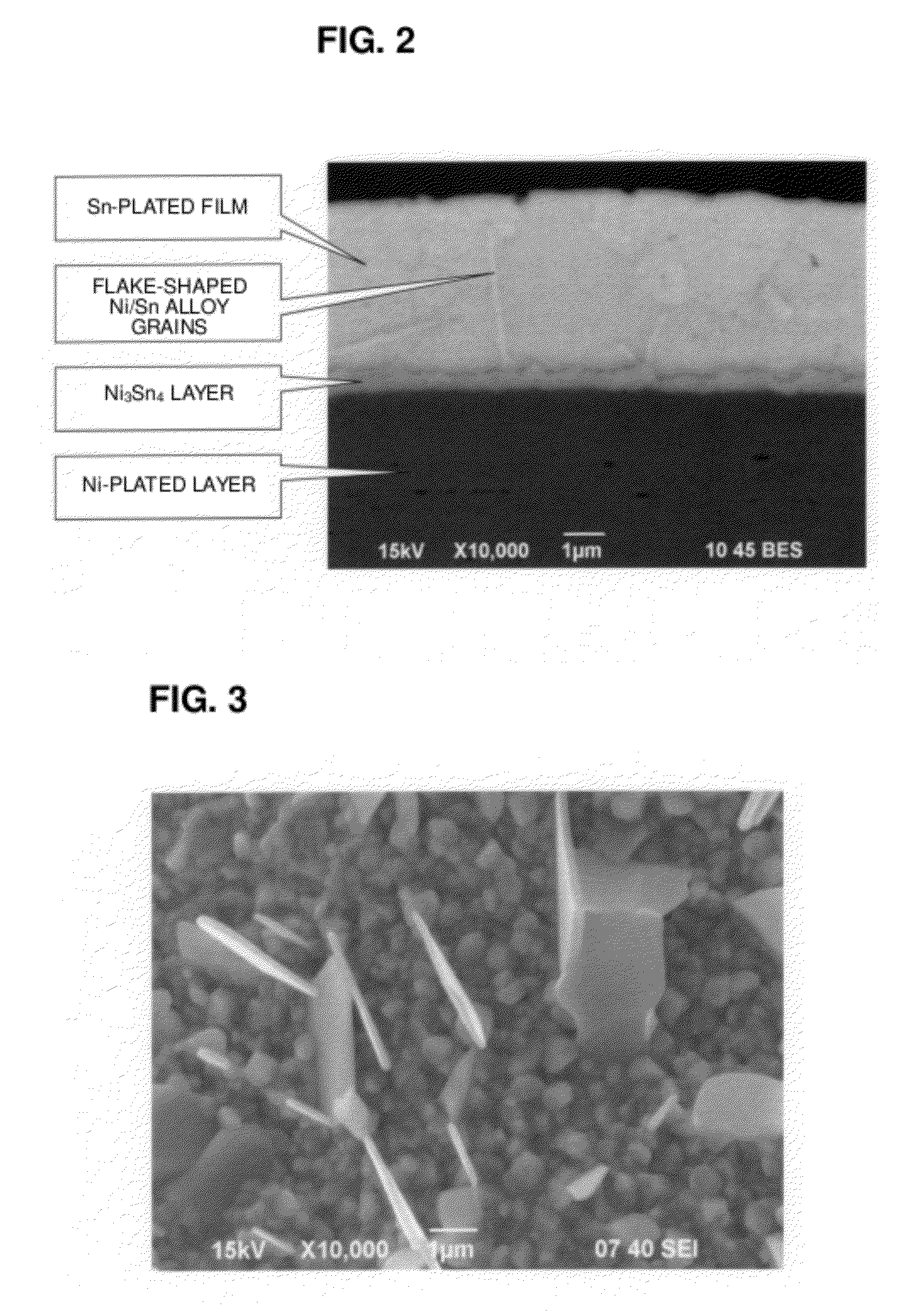
[0046]In the Experimental Example, laminated ceramic capacitors of an Example 1 and Comparative Examples 1 and 2 shown below were produced, and whiskers in films and solder wettability of terminal electrodes were evaluated for those laminated ceramic capacitors.

example 1

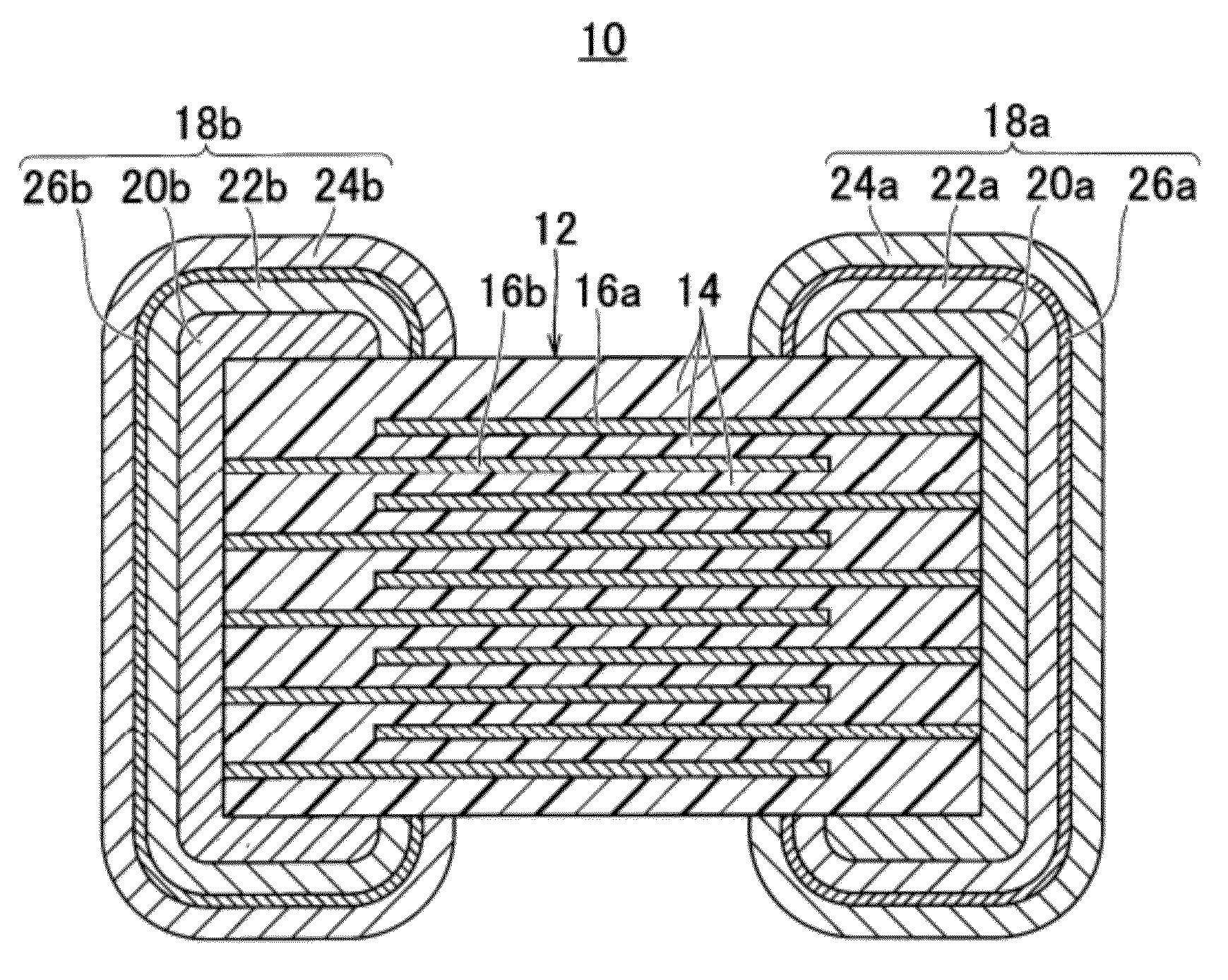
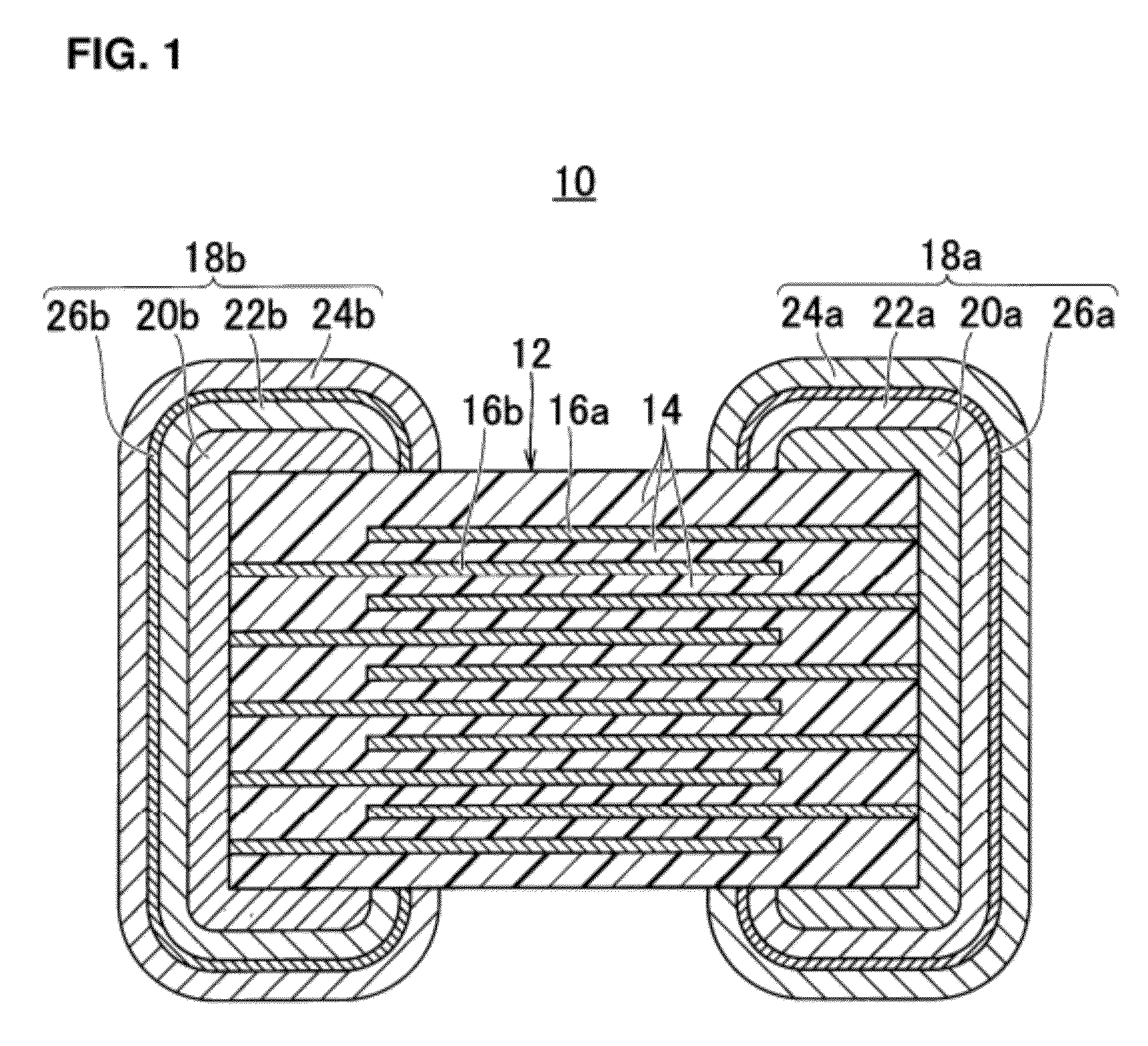
[0047]In Example 1, the laminated ceramic capacitor 10 shown in FIG. 1 was produced by the abovementioned method. In this case, the outside dimensions of the laminated ceramic capacitor 10 were about 2.0 mm (length)×about 1.25 mm (width)×about 1.25 mm (height). A barium titanate-based dielectric ceramic was used as a ceramic layer 14 (dielectric ceramic). Further, Ni was used as a material for the internal electrodes 16a and 16b. Further, Cu was used as a material for the external electrodes 20a and 20b.

[0048]In Example 1, first plated films 22a and 22b and second plated films 24a and 24b were formed under the following conditions.

(1) Plating Bath

[0049]Plating bath for forming the first plated film: a Ni bath generally called a Watts bath was used.

[0050]Plating bath for forming the second plated film: a weak acid Sn plating bath (citric acid-based weak acid bath) with sulfate as a metal salt, citric acid as a complexing agent and one or both of a quaternary ammonium salt and a surf...


PUM

PropertyMeasurementUnit
Fractionaaaaaaaaaa
Structureaaaaaaaaaa
Grain boundaryaaaaaaaaaa

Abstract

An electronic component that prevents or minimizes whiskers or has good solder wettability includes a rectangular solid-shaped electronic component element and external electrodes of terminal electrodes provided at opposed end surfaces of the electronic component element. First plated films including Ni are provided on the surfaces of the external electrodes. Second plated films including Sn defining an outermost layer are arranged so as to cover the first plated films. The second plated films have a polycrystalline structure, and flake-shaped Sn—Ni alloy grains are provided at a Sn crystal grain boundary. Intermetallic compound layers including Ni3Sn4 are provided at interfaces between the first plated films and the second plated films.

Description

BACKGROUND OF THE INVENTION[0001]1. Field of the Invention[0002]The present invention relates to an electronic component, and more particularly, to an electronic component including a Sn-plated film, such as a laminated ceramic capacitor.[0003]2. Description of the Related Art[0004]As a background technique for the present invention, for example, International Publication WO2006 / 134665 discloses a member on which a film including Sn as a main component is formed, a film formation method and a soldering method.[0005]In a terminal for a connector, a lead frame for a semiconductor integrated circuit, and the like, a film is formed on a ground layer formed by Ni-plating or the like using a material having a good solderability. Here, a film is formed by Sn-plating which does not include Pb, instead of plating a Sn—Pb solder which has been conventionally used, in view of environmental concerns. If a Sn-plated film is formed, whisker-like crystals, called whiskers, of Sn tend to develop in...

Claims


Application Information

Patent Timeline
IPC IPC(8): B32B15/01
CPCC23C26/00H01G4/232H01G4/30C23C28/023Y10T428/31678
Inventor OGAWA, MAKOTOMOTOKI, AKIHIROSAITO, ATSUKOMASUKO, KENJIFUJIWARA, TOSHINOBU
Owner MURATA MFG CO LTD
Why Eureka
Try Eureka