Heat treatment method and heat treatment apparatus for heating substrate by irradiating substrate with light

a heat treatment method and heat treatment technology, applied in the direction of optical radiation measurement, furnaces, instruments, etc., can solve the problems of high separation depth, variation in surface temperature to be attained, and extremely difficult to measure the surface temperature of the semiconductor wafer to be treated or processed

Active Publication Date: 2012-11-15
DAINIPPON SCREEN MTG CO LTD
View PDF13 Cites 38 Cited by
  • Summary
  • Abstract
  • Description
  • Claims
  • Application Information

AI Technical Summary

Benefits of technology

[0010]According to one aspect of the present invention, the heat treatment apparatus comprises: a chamber for receiving a substrate therein; a holder for holding the substrate within the chamber; an irradiation part for irradiating the front surface of the substrate held by the holder with light; a quartz window provided in the chamber, for eliminating light having a predetermined wavelength range from light emitted from the irradiation part; a photodetector element provided on the front surface side of the substrate, for receiving radiated light from the front surface; a filter for selectively allowing light having a selective wavelength range included in radiated light directed from the front surface of the substrate toward the photodetector element to pass therethrough, the selective wavelength range being included in the predetermined wavelength range; a back-surface temperature measuring part provided on the back surface side of the substrate, for measuring a temperature of the back surface; a radiated light int...

Problems solved by technology

This results in a junction depth much greater than a required depth, which might constitute a hindrance to good device formation.
However, even if the total energy of flash irradiation is constant, the light energy to be absorbed differs between different emissivities o...

Method used


Image

  • Heat treatment method and heat treatment apparatus for heating substrate by irradiating substrate with light
  • Heat treatment method and heat treatment apparatus for heating substrate by irradiating substrate with light
  • Heat treatment method and heat treatment apparatus for heating substrate by irradiating substrate with light

Examples


Embodiment Construction

[0031]A preferred embodiment according to the present invention will now be described in detail with reference to the drawings.

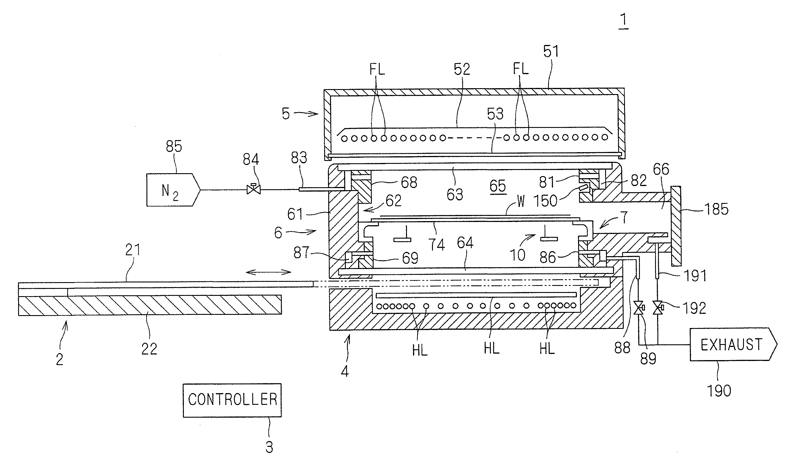
[0032]FIG. 1 is a longitudinal sectional view showing a configuration of a heat treatment apparatus 1 according to the present invention. The heat treatment apparatus 1 according to the preferred embodiment of the present invention is a flash lamp annealer for irradiating a disk-shaped semiconductor wafer W having a diameter of 300 mm and serving as a substrate with a flash of light to heat the semiconductor wafer W. The semiconductor wafer W prior to the transport into the heat treatment apparatus 1 is implanted with impurities. The heat treatment apparatus 1 performs a heating treatment on the semiconductor wafer W to thereby activate the impurities implanted in the semiconductor wafer W.

[0033]The heat treatment apparatus 1 includes a chamber 6 for receiving a semiconductor wafer W therein, a flash heating part 5 including a plurality of built-in flash lam...


PUM


Abstract

After flash irradiation on a semiconductor wafer is started and then the temperatures of front and back surfaces of the semiconductor wafer become equal to each other, the temperature of the back surface of the semiconductor wafer, which has a known emissivity, is measured with a radiation thermometer. The emissivity of the front surface of the semiconductor wafer is calculated based on the intensity of radiated light from a black body having an equal temperature to the temperature of the back surface thereof, and the intensity of radiated light actually radiated from the front surface of the semiconductor wafer. Then, the temperature of the front surface of the semiconductor wafer heated by the flash irradiation is calculated based on the calculated emissivity and the intensity of the radiated light from the front surface of the semiconductor wafer that has been measured after the flash irradiation is started.

Description

BACKGROUND OF THE INVENTION[0001]1. Field of the Invention[0002]The present invention relates to a heat treatment method and a heat treatment apparatus for heating a thin plate-like precision electronic substrate (hereinafter referred to simply as a “substrate”) having a back surface of a known emissivity such as a semiconductor wafer and a glass substrate for a liquid crystal display device by irradiating the substrate with light.[0003]2. Description of the Background Art[0004]In the process of manufacturing a semiconductor device, impurity doping is an essential step for forming a pn junction in a semiconductor wafer. At present, it is common practice to perform impurity doping by an ion implantation process and a subsequent annealing process. The ion implantation process is a technique for causing ions of impurity elements such as boron (B), arsenic (As) and phosphorus (P) to collide against the semiconductor wafer with high acceleration voltage, thereby physically implanting the...

Claims


Application Information

Patent Timeline
IPC IPC(8): H01L21/66F27D11/00H01L21/324
CPCH01L21/67115H01L2924/13091F27B17/0025G01J5/026H01L2924/13055G01J5/0007H01L2924/00
Inventor HASHIMOTO, KAZUYUKIKUSUDA, TATSUFUMI
Owner DAINIPPON SCREEN MTG CO LTD
Why Eureka
Try Eureka