Integrated Circuit (IC) Chip Having Both Metal and Silicon Gate Field Effect Transistors (FETs) and Method of Manufacture

a gate field effect transistor and integrated circuit technology, applied in the direction of semiconductor devices, semiconductor/solid-state device details, diodes, etc., can solve the problems of increasing cooling and packaging costs, increasing chip power consumption, and typical fets being much more complex than switches, so as to reduce short channel effects, reduce pfet vts and channel lengths, and achieve the effect of reducing short channel effects

Inactive Publication Date: 2012-11-22
GLOBALFOUNDRIES INC
View PDF6 Cites 214 Cited by
  • Summary
  • Abstract
  • Description
  • Claims
  • Application Information

AI Technical Summary

Benefits of technology

[0016]It is an aspect of the invention to reduce short channel effects in Integrated Circuits (ICs) without impairing performance;
[0017]It is another aspect of the invention to reduce PFET VTs and channel lengths with minimal increase in PFET short channel effects;
[0018]It is yet another aspect of the invention to reduce short channel effects in low VT, short channel IC PFETs while improving IC performance.
[0019]The present invention relates to Field Effect Transistors (FETs), Integrated Circuit (IC) chips including the FETs, and a method of forming the FETs on ICs. FET locations are defined on a layered semiconductor wafer, preferably a Silicon On Insulator (SOI) wafer. One or more FET locations are defined as silicon gate locations and remaining as Replacement Metal Gate (RMG) FET locations with at least one of each on the IC. Polysilicon gates are formed in all FET locations. Gates in silicon gate locations are tailored, e.g., doped and silicided. Remaining polysilicon gates are replaced with metal in RMG FET locations. FETs are connected together into circuits with RMG FETs being connected to silicon gate FETs.

Problems solved by technology

Thus, notwithstanding the decrease of chip supply voltage, chip power consumption has increased as well.
Both at the chip and system levels, cooling and packaging costs have escalated as a natural result of this increase in chip power.
In practice, however, typical FETs are much more complex than switches.
Also, gate oxide leakage also became a major source static power loss.
However, polysilicon cannot be used with high-k dielectrics.
Also, parasitic circuit resistances reduce performance and complicate design.
Subthreshold current is especially troublesome in achieving what is known as low VT devices, where the VT may be less than 100 millivolts (100 mV).
So, low VT RMGFETs are much more susceptible to short channel effects than equivalent polysilicon gate devices and RMGPFETs are worse than RMGNFETs.
Consequently, especially for complex chips and arrays with a large number of devices, short channel effects can be overwhelming.
When multiplied by the millions and even billions of devices on a state of the art IC, even 100 picoAmps (100 pA) of leakage in each of a million circuits, for example, results in chip leakage on the order of 100 milliAmps (100 mA).
Further, these short channel effects are much worse at operating conditions beyond nominal, e.g., higher supply voltages.
Typically, to achieve low VTs channel doping is selectively reduced or channels are selectively counter doped, either of which degrades device performance.

Method used


Image

  • Integrated Circuit (IC) Chip Having Both Metal and Silicon Gate Field Effect Transistors (FETs) and Method of Manufacture
  • Integrated Circuit (IC) Chip Having Both Metal and Silicon Gate Field Effect Transistors (FETs) and Method of Manufacture
  • Integrated Circuit (IC) Chip Having Both Metal and Silicon Gate Field Effect Transistors (FETs) and Method of Manufacture

Examples


Embodiment Construction

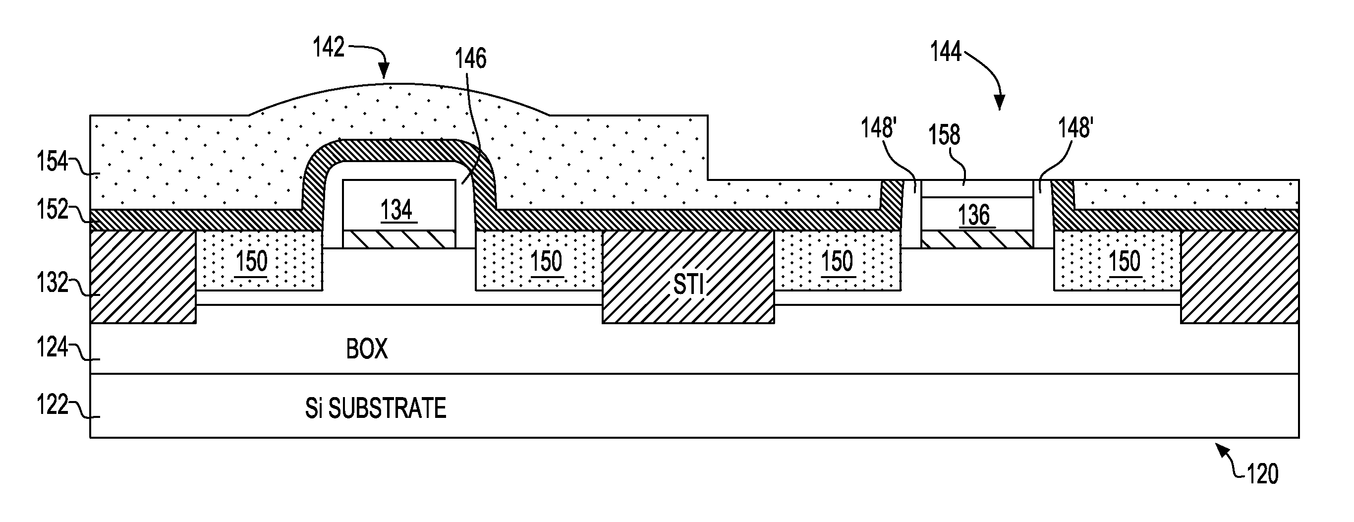
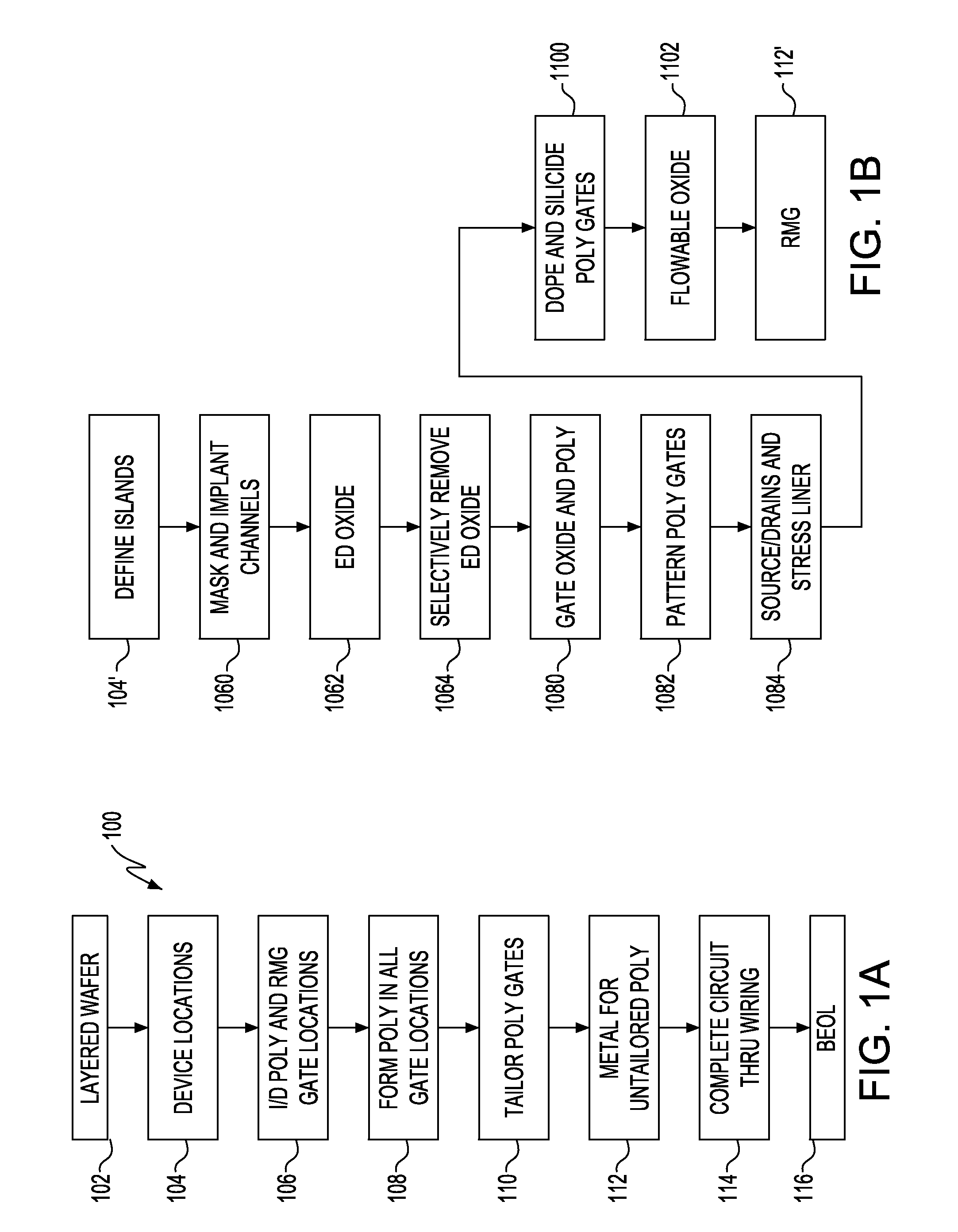
[0031]Turning now to the drawings and, more particularly, FIG. 1A shows a first example of steps in a method 100 for forming semiconductor devices, polysilicon gate Field Effect Transistors (FETs), especially P-type devices, in a Replacement Metal Gate (RMG) FET manufacturing process according to a preferred embodiment of the present invention. Since in RMG nominal PFET devices are not band edged for the gate work function, for certain doping levels, RMGPFETs typically have higher threshold voltages (i.e., the magnitude of the VTs) compared to corresponding polysilicon gate devices with the same doping profile and with the inversion layer thickness (Tinv) matched.

[0032]For a typical state of the art Silicon On Insulator (SOI) process, the PFET metal work function is targeted, best case, at about 100 millivolt (100 mV) from the band edge. Thus, by selectively using a polysilicon gate instead of metal, the same preferred polysilicon gate PFET may be a Super Low VT (SLVT). These prefer...


PUM


Abstract

Field Effect Transistors (FETs), Integrated Circuit (IC) chips including the FETs, and a method of forming the FETs on ICs. FET locations are defined on a layered semiconductor wafer, preferably a Silicon On Insulator (SOI) wafer. One or more FET locations are defined as silicon gate locations and remaining as Replacement Metal Gate (RMG) FET locations with at least one of each on the IC. Polysilicon gates are formed in all FET locations. Gates in silicon gate locations are tailored, e.g., doped and silicided. Remaining polysilicon gates are replaced with metal in RMG FET locations. FETs are connected together into circuits with RMG FETs being connected to silicon gate FETs.

Description

BACKGROUND OF THE INVENTION[0001]1. Field of the Invention[0002]The present invention generally relates to Integrated Circuit (IC) manufacture and more particularly to reducing costs in semiconductor chip manufacture of integrated circuits with short channel Field Effect Transistors (FETs).[0003]2. Background Description[0004]Semiconductor technology and chip manufacturing advances have resulted in a steady decrease of chip feature size to increase on-chip circuit switching frequency (circuit performance) and the number of transistors (circuit density). Shrinking / reducing device or field effect transistor (FET) feature sizes and, correspondingly, device minimum dimensions including horizontal dimensions (e.g., minimum channel length) and vertical dimensions (e.g., channel layer depth, gate dielectric thickness, junction depths and etc.) shrinks device size for increased device density and device performance, as well as reduces device operating conditions, i.e., chip and correspondin...

Claims


Application Information

Patent Timeline
Patent Type & Authority Applications(United States)
IPC IPC(8): H01L29/06H01L21/31
CPCH01L21/82345H01L21/823842H01L27/1203H01L27/0629H01L27/0922H01L21/84H01L2924/0002H01L2924/00H01L29/0653H01L23/5256H01L29/517H01L29/4941H01L29/161H01L29/458H01L29/42364
Inventor KANIKE, NARASIMHULU
Owner GLOBALFOUNDRIES INC
Why Eureka
Try Eureka