Fabricating a contact rhodium structure by electroplating and electroplating composition

a technology of contact rhodium and electroplating, which is applied in the direction of basic electric elements, solid-state devices, transportation and packaging, etc., can solve the problems of increasing parasitic resistance, center voids and seams within the plug, and increasing the difficulty of filling the structure by cvd w process

Inactive Publication Date: 2012-11-22
GLOBALFOUNDRIES INC
View PDF8 Cites 2 Cited by
  • Summary
  • Abstract
  • Description
  • Claims
  • Application Information

AI Technical Summary

Benefits of technology

[0014]The present disclosure also relates to structures obtained by the above disclosed process.

Problems solved by technology

The CVD (chemical vapor deposition) W process is a conformal process which tends to result in center voids and seams within the plug.
Due to the shrinking contact feature sizes and the increase in contact aspect ratio, it becomes more and more challenging to fill the structure by a CVD W process and the increased parasitic resistance.
Furthermore, the shrinking contact feature sizes result in a dramatic increase of parasitic resistance from the overall CVD W plug structure due to the high resistivity of CVD W and the highly resistive Ti / TiN liner stack.
The poor filling of the structure by CVD W process can significantly degrade the performance of the whole chip due to the increased contact resistance with the voids and seams.
It has been used to make electrical contacts due to its low and reliable contact resistance.
Filling of contact vias of 32 nm node and beyond becomes a great challenge for CVD tungsten process due to void formation during the conformal filling, as mentioned above.

Method used


Image

  • Fabricating a contact rhodium structure by electroplating and electroplating composition
  • Fabricating a contact rhodium structure by electroplating and electroplating composition
  • Fabricating a contact rhodium structure by electroplating and electroplating composition

Examples


example 1

[0057]A thin film of 500 nm Rh or less was plated onto Ru-seeded substrate with the Rh plating solution at 50° C. at −2.5 mA / cm2 constant current density and an electrode rotation rate of 100 rpm. The film was then measured with a four-point probe for sheet resistance. The resistivity of the film was calculated with the measured sheet resistance and the film thickness to be 44 micro-ohm-cm. The composition of the film was then measured with the SIMS (secondary ion mass spectroscopy) method and found to have a high level of oxygen, chloride, and sulfur impurity within the Rh. The Rh film was then annealed at 400° C. in forming gas for 4 hours. There is significant grain growth observed from x-ray diffraction, and the Rh resistivity dropped significantly to 9 micro-ohm-cm.

example 2

[0058]A thin film of Rh was plated onto a Ru-seeded substrate with the Rh plating solution at room temperature (varies between 19-24° C.) at −2.5 mA / cm2 constant current density and an electrode rotation rate of 100 rpm. The film was then measured with a four-point probe for sheet resistance. The resistivity of the film was calculated with the measured sheet resistance and the film thickness to be 19 micro-ohm-cm. The composition of the film was then measured with the SIMS method and found to have a much lower level of oxygen and chloride impurity within the Rh, about 2 orders of magnitude lower in both O, Cl, and S concentrations. The Rh film was then annealed at 400° C. in forming gas for 4 hours. There is significant grain growth observed from x-ray diffraction, and the Rh resistivity dropped significantly to 7 micro-ohm-cm.

[0059]See Table 1 for the comparison of the two Rh Examples 1 and 2 plated at different temperatures.

TABLE 1Resistivity of as-plated and post forming gas anne...

example 3

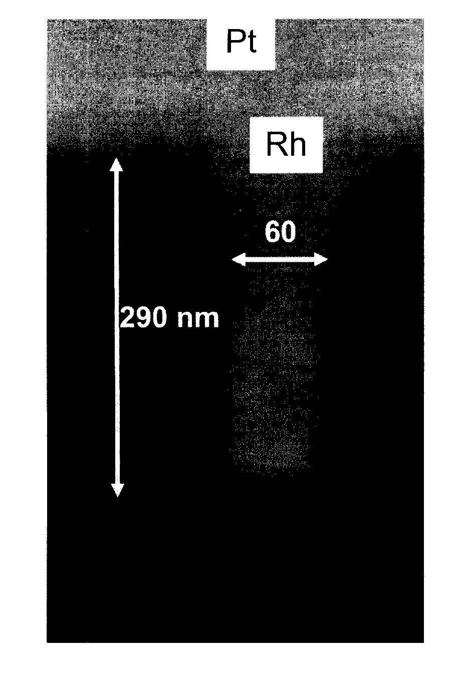
[0060]A structure made of silicide / oxide / ALD TaN / ALD Ru with contact via size of 125 nm×560 nm was plated with Rh. It was plated at room temperature at −2.5 mA / cm2 constant current density and an electrode rotation rate of 100 rpm. The vias are filled with Rh without center voids or center seams.


PUM

PropertyMeasurementUnit
aspect ratioaaaaaaaaaa
dielectric constantaaaaaaaaaa
thickaaaaaaaaaa

Abstract

A contact rhodium structure is fabricated by a process that comprises obtaining a substrate having a dielectric layer thereon, wherein the dielectric layer has cavities therein into which the contact rhodium is to be deposited; depositing a seed layer in the cavities and on the dielectric layer; and depositing the rhodium by electroplating from a bath comprising a rhodium salt; an acid and a stress reducer; and then optionally annealing the structure.

Description

CROSS REFERENCE TO RELATED APPLICATION[0001]This application is a divisional of co-pending application Ser. No. 11 / 737,926, filed on Apr. 20, 2007, and for which priority is claimed under 35 u.s.c. §120; the entire contents of which is are hereby incorporated by reference.DESCRIPTION[0002]1. Technical Field[0003]The present disclosure relates to fabricating a contact metallurgy structure and, in particular, a rhodium structure. The present disclosure is especially significant when filling high aspect ratio submicron structures.[0004]2. Background[0005]Conventional contact plugs are made of CVD (chemical vapor deposition) tungsten (W) for making contact to the front end devices (FEOL). The CVD (chemical vapor deposition) W process is a conformal process which tends to result in center voids and seams within the plug. Due to the shrinking contact feature sizes and the increase in contact aspect ratio, it becomes more and more challenging to fill the structure by a CVD W process and th...

Claims


Application Information

Patent Timeline
Patent Type & Authority Applications(United States)
IPC IPC(8): H01L23/48
CPCC25D3/50C25D5/50H01L21/2885Y10T428/12007H01L23/53242H01L2924/3011H01L21/76877H01L2924/0002H01L2924/00H01L21/288H01L21/768B82Y30/00
Inventor DELIGIANNI, HARIKLIASHAO, XIAOYAN
Owner GLOBALFOUNDRIES INC
Why Eureka
Try Eureka