Logic circuit

a logic circuit and circuit technology, applied in the field of logic circuits, can solve the problems of high potential, long delay time, loss of configuration data stored in the memory portion, etc., and achieve the effects of short start-up time of logic blocks, reduced power consumption, and small amount of off-state current of transistors

Inactive Publication Date: 2012-11-22
SEMICON ENERGY LAB CO LTD
View PDF9 Cites 32 Cited by
  • Summary
  • Abstract
  • Description
  • Claims
  • Application Information

AI Technical Summary

Benefits of technology

[0012]In view of the above problems, it is an object of the present invention to provide a logic circuit which can hold a switching state of the logic circuit even when a power supply potential is not supplied, has short start-up time of a logic block after the power is supplied, can operate with low power consumption, and can easily switch between a NAND circuit and a NOR circuit.
[0013]In one embodiment of the present invention, a transistor with sufficiently small off-state current is used for switching between a NAND circuit and a NOR circuit. The transistor can be formed using, for example, an oxide semiconductor which is a wide bandgap semiconductor as a material which allows a sufficient reduction in off-state current of the transistor. When such a semiconductor material which allows a sufficient reduction in off-state current of the transistor is used, a switching state of the logic circuit can be held even when a power supply potential is not supplied.
[0014]The off-state current per micrometer of channel width of the transistor is 1×10⁻¹⁸ A or less, preferably 1×10⁻²¹ A or less, more preferably 1×10⁻²⁴ A or less. With the use of such a transistor, a memory cell with excellent data holding characteristics and low power consumption can be manufactured.
[0019]In one embodiment of the present invention, the above oxide semiconductor contains at least one element selected from In, Ga, Sn, and Zn. With the use of such an oxide semiconductor for a channel region of a transistor, the amount of off-state current of the transistor can be small. Thus, when the transistor including an oxide semiconductor is applied to a logic circuit, power consumption can be reduced.
[0020]According to one embodiment of the present invention, it is possible to provide a logic circuit which can hold a switching state of the logic circuit even when a power supply potential is not supplied, has short start-up time of a logic block after the power is supplied, can operate with low power consumption, and can easily switch between a NAND circuit and a NOR circuit.

Problems solved by technology

In the case where a volatile memory such as SRAM is included in the memory portion of the programmable switch, configuration data stored in the memory portion is lost when the supply of power supply voltage is stopped.
Therefore, there is a long delay time from the start of supply of power to operation of the logic block.
However, a high potential needs to be applied because electrons need to be injected into a floating gate in data writing; accordingly, it takes a long time to write data.
Therefore, there is a problem of increased power consumption.
Moreover, there is a problem in that a gate insulating layer of the floating gate deteriorates because of tunneling current generated in the data writing.

Method used


Image

  • Logic circuit
  • Logic circuit
  • Logic circuit

Examples


embodiment 1

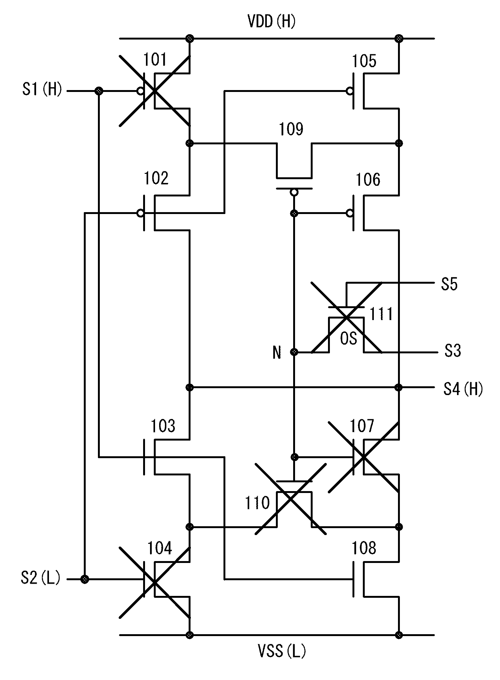
[0050]In this embodiment, a logic circuit capable of switching between a NAND circuit and a NOR circuit according to one embodiment of the present invention will be described with reference to FIG. 1.

[0051]In the logic circuit illustrated in FIG. 1, a first transistor 101, a second transistor 102, a third transistor 103, and a fourth transistor 104 are connected in series. A fifth transistor 105, a sixth transistor 106, a seventh transistor 107, and an eighth transistor 108 are connected in series. One of a source and a drain of the first transistor 101 and one of a source and a drain of the fifth transistor 105 are connected to a high potential power supply line VDD. One of a source and a drain of the fourth transistor 104 and one of a source and a drain of the eighth transistor 108 are connected to a low potential power supply line VSS. A gate of the first transistor 101, a gate of the third transistor 103, and a gate of the eighth transistor 108 are connected to a first signal li...

embodiment 2

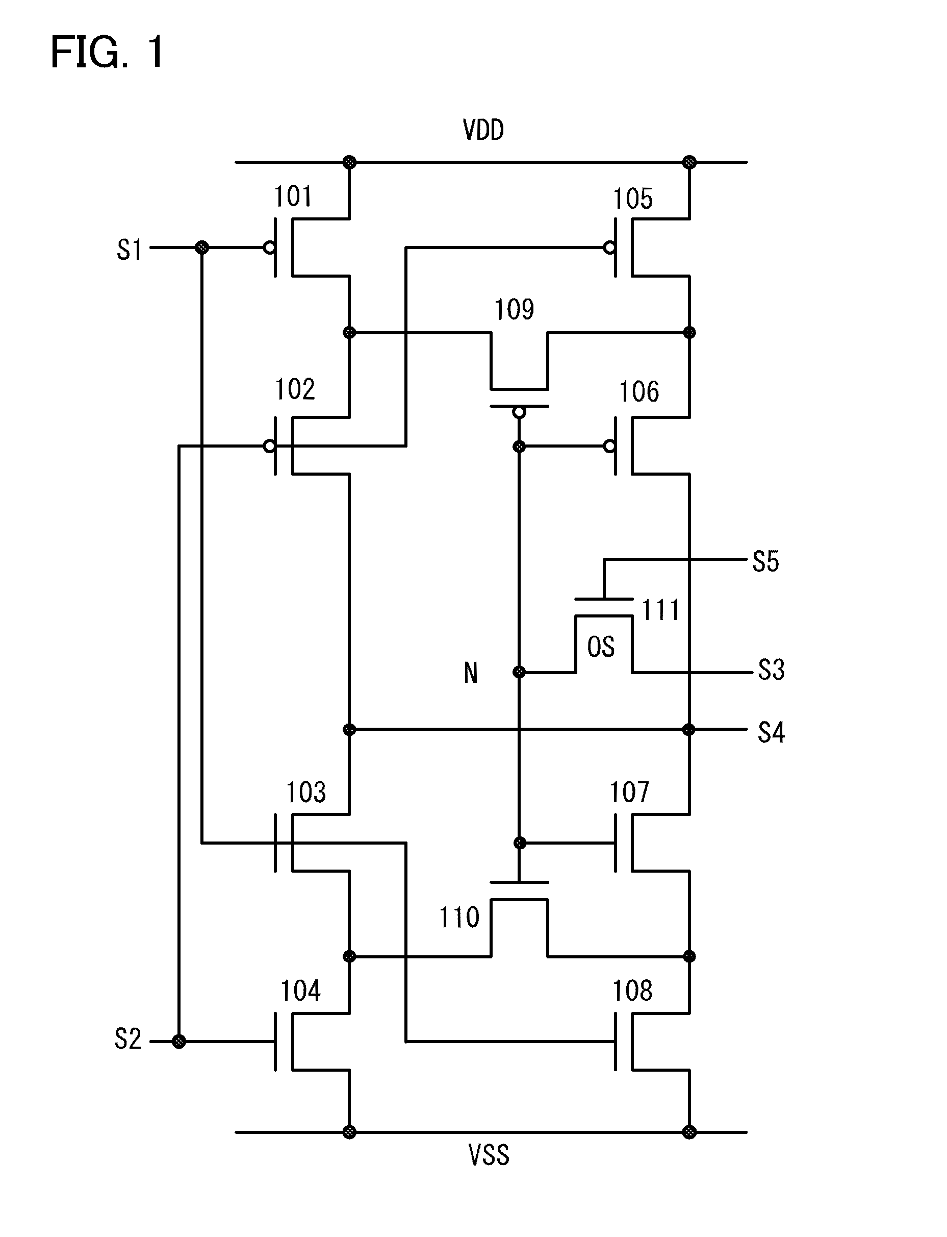
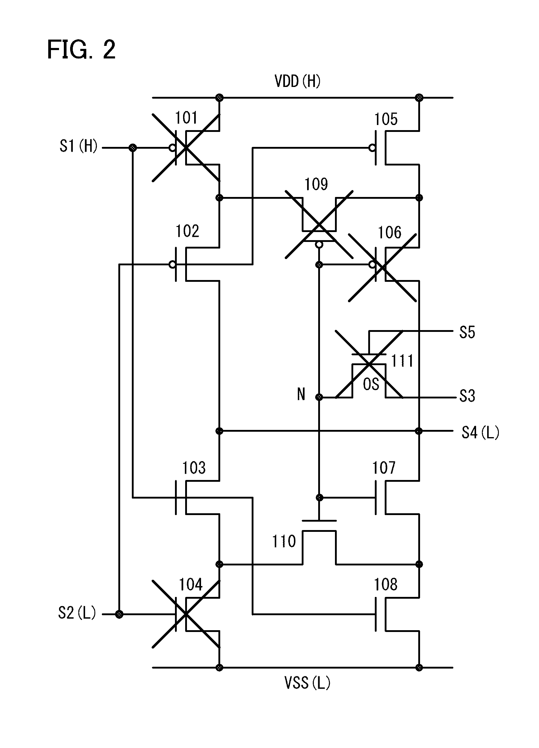
[0072]In this embodiment, a method for manufacturing the transistors of the logic circuit in Embodiment 1 will be described with reference to FIGS. 4A to 4D, FIGS. 5A and 5B, FIGS. 6A to 6C, and FIGS. 7A and 7B. A method for manufacturing the transistor 111, the transistor 107, and the transistor 106 of the logic circuit illustrated in FIG. 1 will be described as an example. Note that in FIGS. 4A to 4D, FIGS. 5A and 5B, FIGS. 6A to 6C, and FIGS. 7A and 7B, a cross-sectional view taken along line A-B corresponds to a cross-sectional view of a region where the transistor 111 including an oxide semiconductor film, the n-channel transistor 107, and the p-channel transistor 106 are formed and where the transistor 111 is stacked over the n-channel transistor 107 and the p-channel transistor 106, and a cross-sectional view taken along line C-D corresponds to a cross-sectional view of the node N at which the one of the source electrode and the drain electrode of the transistor 111 including...

embodiment 3

[0215]In this embodiment, the field-effect mobility of the transistor including an oxide semiconductor film, which is described in the above embodiments, is theoretically calculated, and the transistor characteristics are calculated from the field-effect mobility.

[0216]The actually measured field-effect mobility of an insulated gate transistor can be lower than its ideal mobility because of a variety of reasons; this phenomenon occurs not only in the case of using an oxide semiconductor. One of the causes for the lower mobility is a defect inside a semiconductor or a defect at an interface between the semiconductor and an insulating film. When a Levinson model is used, the field-effect mobility on the assumption that no defect exists inside the semiconductor can be calculated theoretically.

[0217]Assuming that the ideal mobility and the measured field-effect mobility of a semiconductor are μ0 and μ, respectively, and a potential barrier (such as a grain boundary) exists in the semico...


PUM


Abstract

A logic circuit is provided which can hold a switching state of the logic circuit even when a power supply potential is not supplied, has short start-up time of a logic block after the power is supplied, can operate with low power consumption, and can easily switch between a NAND circuit and a NOR circuit. Switching between a NAND circuit and a NOR circuit is achieved by switching a charge holding state at a node through a transistor including an oxide semiconductor. With the use of an oxide semiconductor material which is a wide bandgap semiconductor for the transistor, the off-state current of the transistor can be sufficiently reduced; thus, the state of charge held at the node can be non-volatile.

Description

BACKGROUND OF THE INVENTION[0001]1. Field of the Invention[0002]The present invention relates to a logic circuit and a semiconductor device including the logic circuit. Further, the present invention relates to an electronic device including the semiconductor device.[0003]In this specification, a semiconductor device generally means a device which can function by utilizing semiconductor characteristics, and an electro-optical device, a light-emitting display device, a large scale integrated circuit, and an electronic device are all semiconductor devices.[0004]2. Description of the Related Art[0005]In general, a circuit configuration of a semiconductor integrated circuit typified by a large scale integration (LSI) circuit is fixed at the time of manufacture and cannot be changed after the manufacture. In contrast, a semiconductor integrated circuit called a programmable logic device (PLD) has a structure in which unit logic blocks each including a plurality of logic circuits are elec...

Claims


Application Information

Patent Timeline
Patent Type & Authority Applications(United States)
IPC IPC(8): H03K19/0948H03K19/094
CPCH03K19/0948H03K19/017581H03K19/17772H03K19/1776G11C16/0483H01L21/82H10B63/30
Inventor TAKEWAKI, YOSHIYA
Owner SEMICON ENERGY LAB CO LTD
Why Eureka
Try Eureka