Transfer method, method for manufacturing semiconductor device, and semiconductor device

a technology of semiconductor devices and transfer methods, applied in the direction of semiconductor devices, basic electric elements, electrical appliances, etc., can solve the problems of difficult even reduction of manufacturing costs, large initial investment, and inability to achieve desired performance of thin-film transistors, so as to reduce the number of transfers, prevent displacement, and reduce the effect of the number of transfers

Inactive Publication Date: 2012-11-29
SHARP KK
View PDF16 Cites 26 Cited by
  • Summary
  • Abstract
  • Description
  • Claims
  • Application Information

AI Technical Summary

Benefits of technology

[0090]As described above, by forming depressed portions in advance in that surface of a semiconductor substrate on which the semiconductor elements are to be formed, bonding together that surface of the semiconductor substrate on which the semiconductor elements are to be formed and an intermediate transfer substrate, and then grinding the semiconductor substrate from a bottom wall side of the depressed portions, the semiconductor elements, such as single-crystal silicon films or semiconductor devices made of single-crystal silicon fabricated into a single-crystal silicon substrate, can be transferred; moreover, the elements can be separated with one transfer. For this reason, according to each of the methods described above, the elements can be separated without an increase in the number of transfers, and the element sections including the semiconductor elements can be transferred from the semiconductor substrate to the final transfer substrate with two transfers. This makes it possible to make the number of transfers smaller than in the conventional case.
[0091]Further, a reduction in the number of transfers makes it possible to prevent displacements from being caused by repetition of transfers. Moreover, only the element sections that need to be transferred can be selectively transferred to the final transfer substrate without using vacuum contact by vacuum equipment. Therefore, there is no fear of leakage of vacuum contact or of rotation or displacement during vacuum contact.
[0092]Furthermore, according to each of the methods described above, the element sections that need to be transferred to the final transfer substrate are transferred to the final transfer substrate by being joined to the final transfer substrate. Therefore, there does not occur a prominence of a soft resin due to the burial of semiconductor elements in the soft resin as would have conventionally occurred. For this reason, the element sections can be transferred with a high degree of positioning accuracy.
[0093]Further, according to each of the methods described above, the element sections that need to be transferred to the final transfer substrate can be selectively transferred dispersedly to the final transfer substrate. Therefore, the element sections can be transferred to the final transfer substrate at a desired pitch, and the efficiency in the use of the semiconductor substrate can be improved. Therefore, throughput and transfer accuracy can be increased.
[0094]Further, according to each of the methods described above, the efficiency in the use of the semiconductor substrate can be improved, and the number of transfers can be made smaller than in the conventional case. Therefore, by manufacturing a semiconductor apparatus by using any one of the methods described above, the cost of manufacturing the semiconductor apparatus can be reduced. Further, since neither a special apparatus nor expensive facilities are required, the cost of initial investment can be held down.
[0095]Therefore, each of the methods and configurations described above realizes high-accuracy transfer with few displacements, and can achieve an improvement in yield and a reduction in cost due to shortening of the manufacturing process. Further, this also makes it possible to improve the processing capability (takt time) of the manufacturing process.

Problems solved by technology

However, conventional TFT processes, such as a-Si (amorphous silicon) process and a poly-Si (polycrystalline silicon) process, are unable to give a TFT (thin-film transistor) with desired performance and, what is even worse, require giant vacuum equipment, a laser crystallization apparatus, an exposure machine, etc., thus making it difficult to even reduce manufacturing cost.
Therefore, along with the increase in size of glass substrates (10th-generation size: 3.1 m×2.9 m), this method requires expensive apparatuses such as giant vacuum equipment and a laser crystallization apparatus, thus requiring huge initial investments.
However, in such a case of pixel TFTs where the semiconductor elements are divided into several millions of chips (several tens of millimeters in size) and the chips are bonded, the foregoing method is unrealistic in terms of both throughput and handling.
Further, as mentioned above, in the case of use of the Smart-Cut method for the transfer, the whole Si substrate is inevitably heated.
This makes it difficult to selectively transfer only the semiconductor elements that need to be transferred.

Method used


Image

  • Transfer method, method for manufacturing semiconductor device, and semiconductor device
  • Transfer method, method for manufacturing semiconductor device, and semiconductor device
  • Transfer method, method for manufacturing semiconductor device, and semiconductor device

Examples


embodiment 1

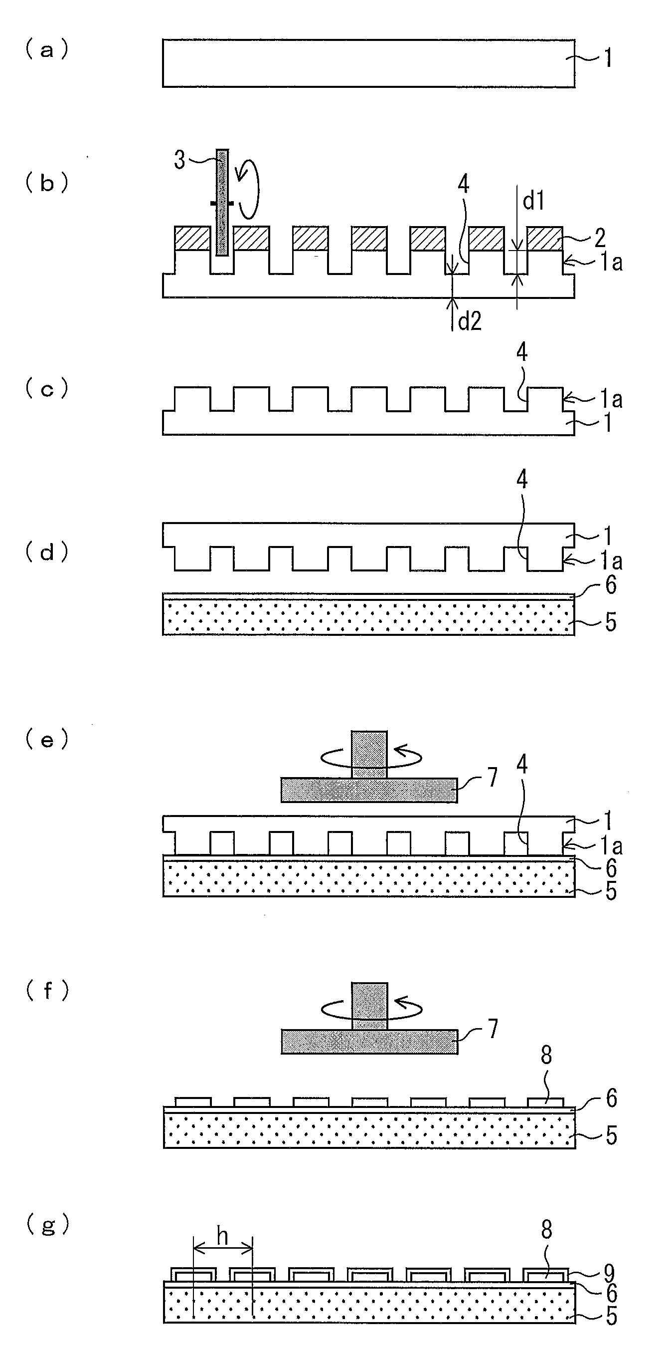
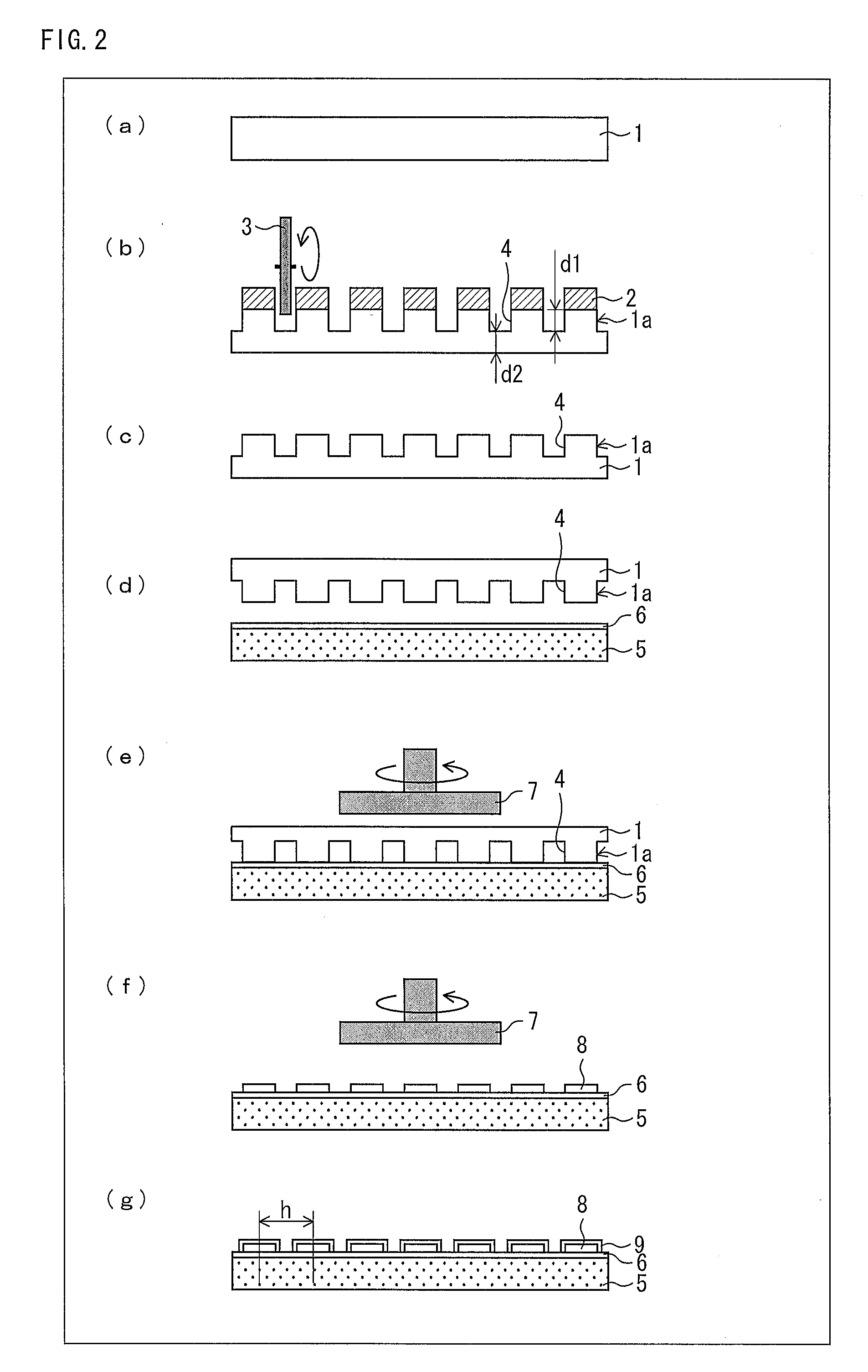
[0132]An embodiment of the present invention is described below with reference to FIGS. 1 through 7.

[0133]A method for manufacturing a semiconductor apparatus according to the present embodiment is a method for manufacturing a semiconductor apparatus by using a so-called device transfer technique for transferring semiconductor elements from a semiconductor substrate serving as a base substrate to a final substrate (final transfer substrate, mounting substrate) on which the semiconductor elements are to be finally mounted.

[0134]The semiconductor substrate may be a substrate (semiconductor wafer) made of a semiconductor material, such as a Si substrate, an SOI (Silicon On Insulator) substrate, a GaN substrate, or a GaAs substrate, for example, or may be a substrate obtained by forming a semiconductor film made of a crystal of Si, GaN, GaAs, or the like on an insulating substrate such as a sapphire substrate.

[0135]Further, examples of the final substrate include insulating substrates s...

embodiment 2

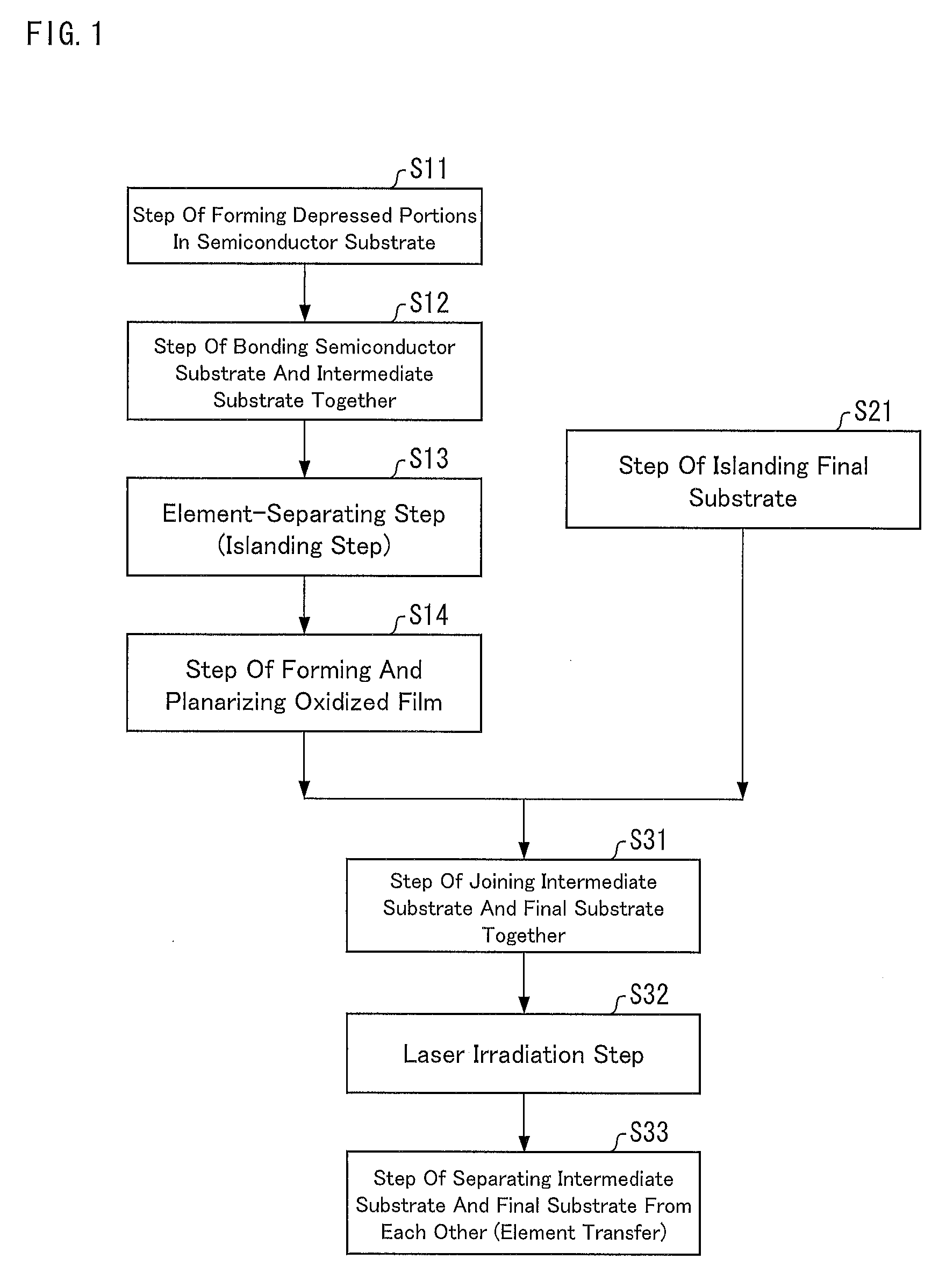
[0253]Another embodiment of the present invention is described below with reference to FIG. 8 through (a) to (c) of FIG. 10.

[0254]FIG. 8 is a flow chart schematically showing main steps of a method for manufacturing a semiconductor apparatus according to the present embodiment. Further, FIG. 9 is a set of cross-sectional views (a) to (f) showing steps from S11 to S13 of FIG. 8 in the order in which they are executed. FIG. 10 is a set of cross-sectional views (a) to (c) showing steps from S31 to S33 of FIG. 8 in the order in which they are executed. The steps shown in S21 of FIG. 8 are identical to the steps shown in S21 of FIG. 1, and the cross-sectional views showing the steps in S21 in the order in which they are executed are identical to (a) to (c) of FIG. 3. Therefore, the steps shown in S21 of FIG. 8 in the order in which they are executed are omitted from the illustrations.

[0255]>

[0256]First, a method for manufacturing a semiconductor apparatus according to the present embodim...

embodiment 3

[0294]Another embodiment of the present invention is described below with reference to FIG. 11 through (a) to (c) of FIG. 13.

[0295]FIG. 11 is a flow chart schematically showing main steps of a method for manufacturing a semiconductor apparatus according to the present embodiment. Further, FIG. 12 is a set of cross-sectional views (a) to (h) showing steps from S41 to S46 of FIG. 11 in the order in which they are executed. FIG. 13 is a set of cross-sectional views (a) to (c) showing steps from S51 to S53 of FIG. 11 in the order in which they are executed. The steps shown in S21 of FIG. 11 are identical to the steps shown in S21 of FIG. 1, and the cross-sectional views showing the steps in S21 in the order in which they are executed are identical to (a) to (c) of FIG. 3. Therefore, the steps shown in S21 of FIG. 11 in the order in which they are executed are omitted from the illustrations.

[0296]>

[0297]First, a method for manufacturing a semiconductor apparatus according to the present ...


PUM


Abstract

After depressed portions (4) have been formed in advance in that surface of a Si substrate (1) on which Si single films (8) are to be formed, that surface of the Si substrate (1) on which the Si single films are to be formed and an intermediate substrate (5) are bonded together, and elements are separated from each other by grinding the Si substrate (1) from the bottom wall side of the depressed portions (4).

Description

TECHNICAL FIELD[0001]The present invention relates to a transfer method for transferring semiconductor elements such as single-crystal silicon from a semiconductor substrate to a final substrate on which the semiconductor elements are to be finally mounted, a method for manufacturing a semiconductor apparatus by using such a transfer method, and a semiconductor apparatus.BACKGROUND ART[0002]In recent years, displays for computers, television apparatuses, etc. have been growing in size and, at the same time, have been required to be manufactured with superhigh performance at low cost.[0003]For manufacturing of displays with superhigh performance at low cost, it is necessary to achieve both TFTs (thin-film transistors) comparable in performance to single-crystal silicon (the word “silicon” being hereinafter abbreviated as “Si”) and a reduction in manufacturing cost.[0004]However, conventional TFT processes, such as a-Si (amorphous silicon) process and a poly-Si (polycrystalline silico...

Claims


Application Information

Patent Timeline
Patent Type & Authority Applications(United States)
IPC IPC(8): H01L21/762H01L27/12
CPCH01L21/2007H01L21/78H01L27/1266
Inventor MITANI, MASAHIRO
Owner SHARP KK
Why Eureka
Try Eureka