Solar cell and solar cell manufacturing method

Inactive Publication Date: 2012-12-06
FUJIFILM CORP
View PDF7 Cites 15 Cited by
  • Summary
  • Abstract
  • Description
  • Claims
  • Application Information

AI Technical Summary

Benefits of technology

[0045]The solar cell of the invention is a module type in which thin-film solar cells including a light absorbing layer (photoelectric conversion layer) made of a compound semiconductor such as CIGS are joined in series on a single substrate. The substrate used has an aluminum (Al) layer formed on a surface of a metallic base and an anodized aluminum film serving as an insulation layer. A ferritic stainless steel is used for the base of the substrate.
[0046]According to the solar cell of the invention in which a ferritic stainless steel is used for the base, cracking and delamination of the anodized film serving as the insulation layer can be suppressed even if the light absorbing layer is formed at a high temperature of 500 deg C. or more, whereby good insulation properties can be maintained.
[0047]In cases where an austenitic stainless steel or a low-carbon steel is used for the metallic base of the substrate of the same structure, the light absorbing layer may partially come off in the shape of spots or have cracks, leading to a decrease in the conversion efficiency of the solar cell. In contrast, the solar cell of the invention which uses a ferritic stainless steel for the base can suppress occurrence of such partial peeling, whereby the solar cell obtained has good conversion efficiency.
[0048]As described above, the invention is capable of maintaining high insulation properties and a high strength even after the step at a temperature of 500 deg C. or more. In other words, a manufacturing step at a high temperature of 500 deg C. or more is possible and the light absorbing layer made of a compound semiconductor can be formed at a film deposition temperature of 500 deg C. or more.
[0049]The compound semiconductor making up the light absorbing layer should be formed at a high temperature so that photoelectric conversion properties may be improved. Therefore, according to the invention, a solar cell having a light absorbing layer with improved photoelectric conversion properties can be obtained by film deposition at a temperature of 500 deg C. or more.
[0050]Moreover, the invention is capable of suppressing cracking and partial peeling of the anodized film serving as the insulation layer and the light absorbing layer even in a case where the solar cell is manufactured by a roll-to-roll process and a bending force is repeatedly applied by the rollers onto the substrate and the solar cell during manufacturing. As a result, a sound solar cell that is free of cracking and partial peeling of the substrate and light absorbing layer can be achieved.

Problems solved by technology

However, these techniques easily cause pinholes and cracks and have essential problems in consistently preparing a large-area thin-film insulation layer.
Once cracking occurs, the insulation properties are deteriorated and particularly the leakage current is increased, leading to unsatisfactory photoelectric conversion efficiency.
Therefore, handling of solar cells using aluminum substrates is to be strictly restricted also during the manufacture thereof.
This makes it difficult for such solar cells using aluminum substrates to be applied to outdoor solar cell units.

Method used


Image

  • Solar cell and solar cell manufacturing method
  • Solar cell and solar cell manufacturing method
  • Solar cell and solar cell manufacturing method

Examples


working example 1

[0263]Next, the invention is described in further detail by referring to specific examples of the solar cell of the invention.

[0264]In Table 1 below, A to E shown in the metallic base column indicate the structure of the substrate, and the details thereof will now be described.

[0265]The following describes the metallic bases A to E, anodization, and annealing.

Metallic Base A (Inventive Substrate)

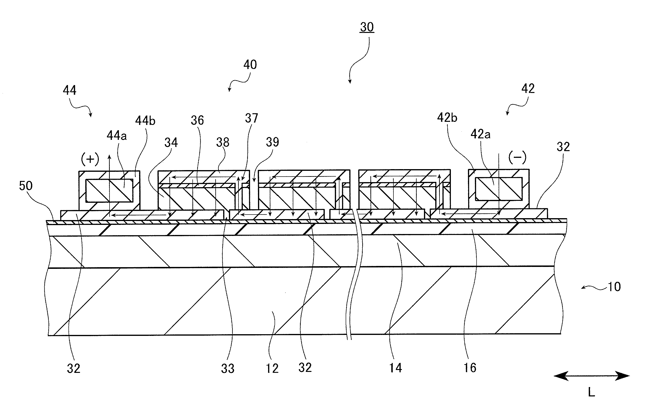
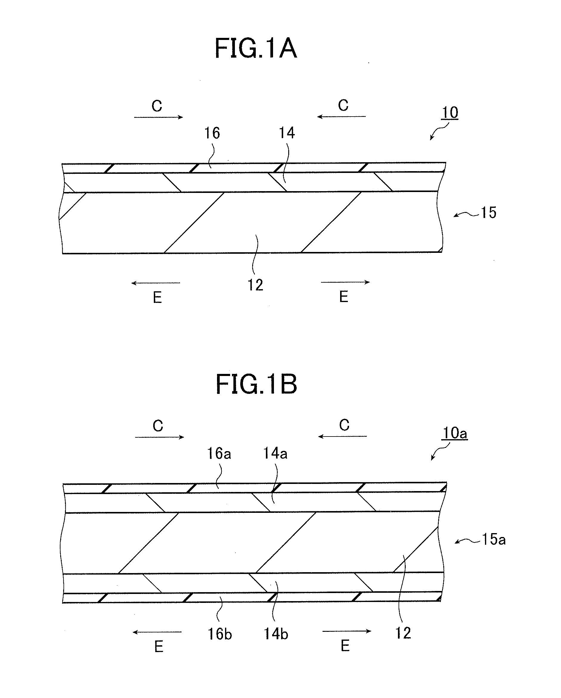
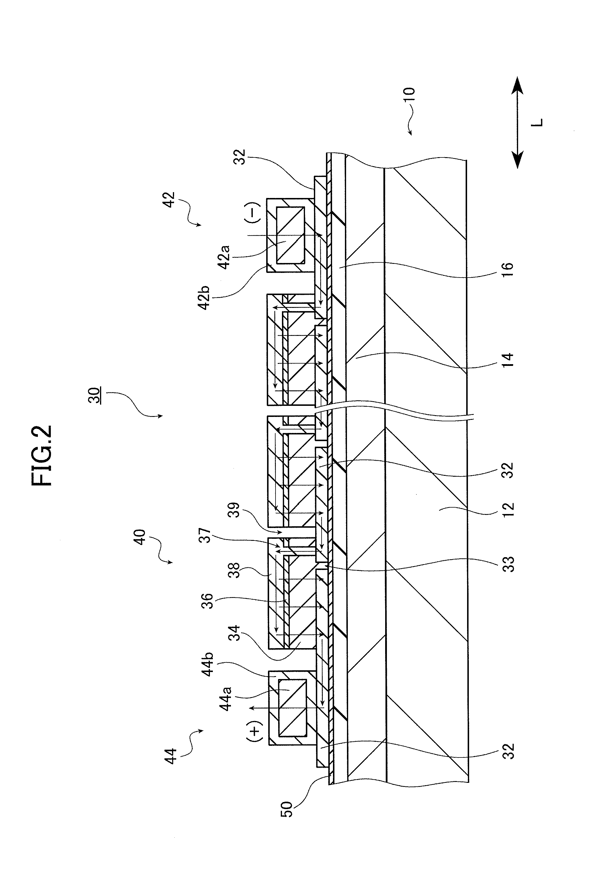
[0266]A commercially available ferritic stainless steel (material type: SUS430) and high-purity aluminum (aluminum purity: 4N) were pressurized and bonded by cold rolling to prepare a two-layer clad material including a base 12 (ferritic stainless steel) with a reduced thickness of 50 micrometers and an Al layer 14 with a reduced thickness of 30 micrometers. The clad metallic base was thus obtained.

[0267]The back surface (opposite from the Al layer 14) and the end surfaces of the base 12 in the two-layer clad material were then covered with a masking film. Next, ultrasonic cleaning was perfo...


PUM


Abstract

A solar cell of a module type in which thin-film solar cells having a light absorbing layer made of a compound semiconductor are joined in series on a single substrate. The substrate includes a base made of a ferritic stainless steel, an aluminum layer formed on at least one surface of the base, and an insulation layer having a porous structure obtained by anodizing a surface of the aluminum layer. The insulation layer exhibits compressive stress at room temperature.

Description

TECHNICAL FIELD[0001]The present invention relates to a solar cell which has a light absorbing layer made of a compound semiconductor such as a CIGS compound on a metallic substrate having an insulation layer formed therein and exhibits excellent insulation properties and photoelectric conversion efficiency. The invention also relates to a method of manufacturing such a solar cell.BACKGROUND ART[0002]Silicon solar cells using bulky monocrystalline or polycrystalline silicon or thin-film amorphous silicon have conventionally been mainly employed but compound semiconductor solar cells which do not depend on silicon are recently under research and development.[0003]Bulky materials such as GaAs and thin-film materials such as CIS (Cu—In—Se) and CIGS (Cu—In—Ga—Se) including a group Ib element, a group IIIb element, and a group VIb element are known for the compound semiconductor solar cells. CIS and CIGS materials are reported to have high optical absorptance and high photoelectric conve...

Claims


Application Information

Patent Timeline
IPC IPC(8): H01L31/042H01L31/18
CPCH01L31/022425H01L31/0322H01L31/046Y02E10/541H01L31/0323H01L31/0392H01L31/022441H01L31/03923Y02P70/50
Inventor YUYA, SHIGENORISATO, KEIGONAKAYAMA, RYUICHIKAITO, RYOZOMURAKAMI, NAOKI
Owner FUJIFILM CORP
Why Eureka
Try Eureka