

Power semiconductor device
- Summary
- Abstract
- Description
- Claims
- Application Information
AI Technical Summary
Benefits of technology
Problems solved by technology
Method used
Image


Examples
first embodiment
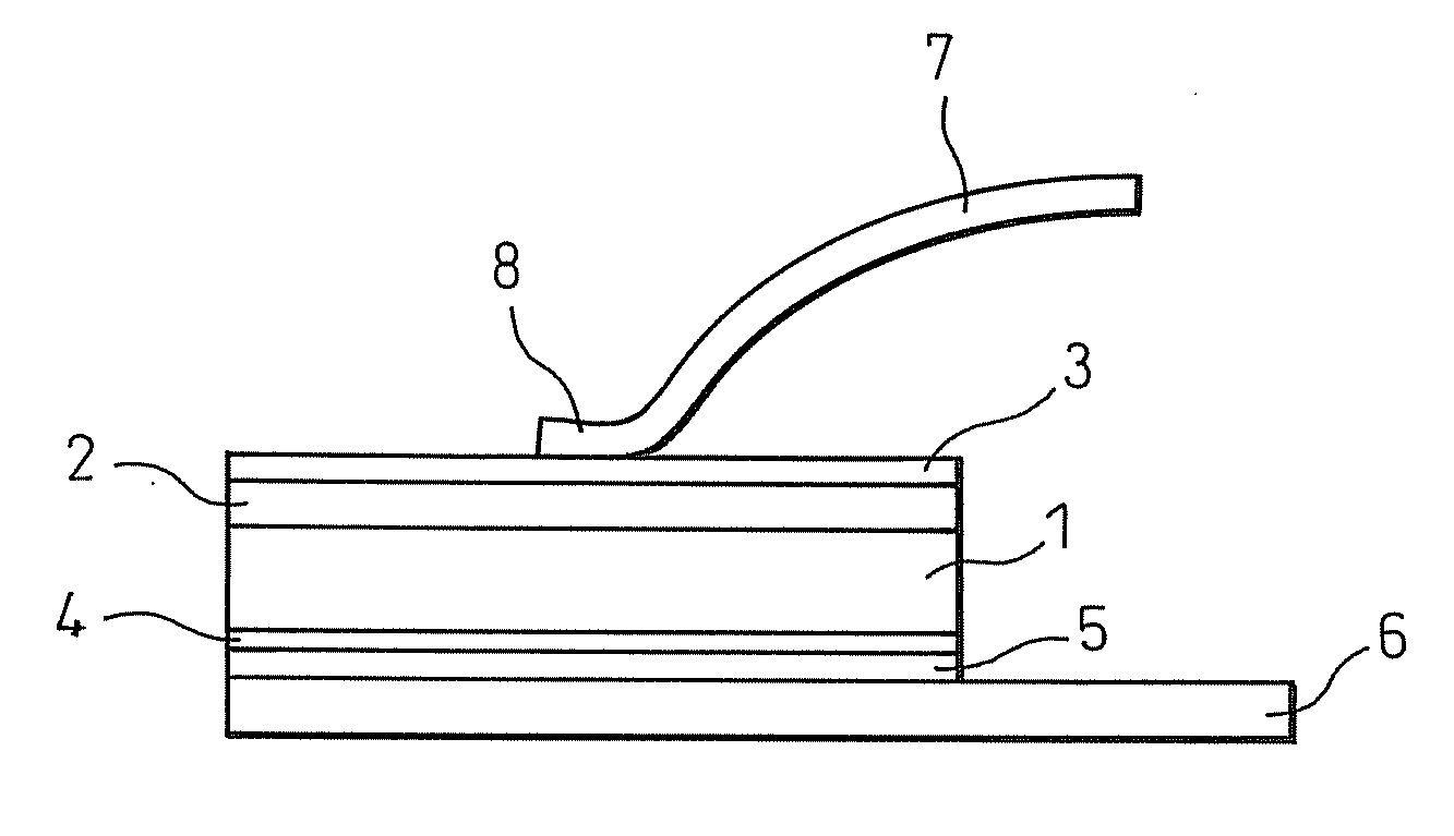
[0039]FIG. 1 is a diagram showing the configuration of the present invention. A silicon carbide substrate (coefficient of linear expansion: 4.2×10⁻⁶ / K) designated by symbol 1 of FIG. 1 is 4H n-type. The silicon carbide substrate 1 is a 5 mm×5 mm square having a thickness of about 200 μm. A silicon carbide homoepitaxial layer designated by symbol 2 of FIG. 1 has a thickness of around 10 μm. A 1 μm thick molybdenum film (coefficient of linear expansion: 4.9×10⁻⁶ / K) 3 is formed on the epitaxial layer 2 by sputtering to form a schottky electrode. Further, symbol 4 of FIG. 1 is a 0.3 μm thick nickel film formed by sputtering. After the nickel film 4 has been formed, heat treatment is performed at 1000° C. for about 2 min to form an ohmic junction on the rear surface of the silicon carbide substrate (semiconductor device substrate) 1. In addition, molybdenum film metal (film) 5 is formed on rear surface of the nickel film 4 by sputtering to a thickness of about 2 μm.
[0040]A bus bar (conne...
second embodiment
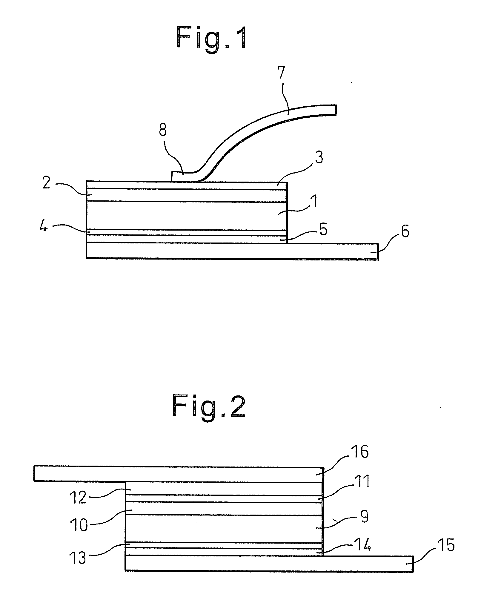
[0045]FIG. 2 is a diagram showing the configuration of the present invention. An n-type GaN substrate (coefficient of thermal expansion: 5.6×10⁻⁶ / K) designated by symbol 9 of FIG. 2 is the size of a 3 mm×3 mm square having a thickness of about 300 μm. The thickness of a GaN homoepitaxial layer (film) designated by symbol 10 of FIG. 2 is about 10 μm. A 0.2 μm thick palladium film (coefficient of linear expansion: 11.8×10⁻⁶ / K) 11 is formed on the epitaxial layer by sputtering to form a schottky electrode. On this is formed by sputtering a 2 μm thick tungsten electrode (coefficient of linear expansion: 4.3×10⁻⁶ / K) 12.
[0046]Further, symbol 13 of FIG. 2 is a titanium and gold multilayer film formed by sputtering to a thickness of 0.3 μm. After formation of the multilayer film 13, heat treatment is performed at 900° C. for about 30 sec to form an ohmic junction on the rear surface of the GaN substrate. In addition, a tungsten metal (film) 14 is formed on the surface of the multilayer film...
PUM
 Abstract
Description
Claims
Application Information