Semiconductor device and method for manufacturing the same

a semiconductor device and semiconductor technology, applied in the direction of semiconductor devices, electrical equipment, transistors, etc., can solve the problems of inconvenient drain current flow even at negative voltage, difficult control of the circuit, and the power consumption of the semiconductor device, so as to improve the on-state characteristics, high-speed operation, and quick response

Active Publication Date: 2012-12-20
SEMICON ENERGY LAB CO LTD
View PDF9 Cites 109 Cited by
  • Summary
  • Abstract
  • Description
  • Claims
  • Application Information

AI Technical Summary

Benefits of technology

[0010]An improvement in the on-state characteristics (e.g., on-state current and field effect mobility) of a transistor leads to quick response to an input signal and high-speed operation of a semiconductor device; thus, a semiconductor device with higher performance can be achieved. On the other hand, a sufficiently low off-state current is needed to reduce power consumption of a semiconductor device. That is, required electric characteristics of a transistor vary with uses and purposes of the transistor, and it is profitable to control the electric characteristics more accurately.

Problems solved by technology

If the threshold voltage of the transistor is negative, the transistor tends to be in a so-called normally-on state, in which current flows between the source electrode and the drain electrode even when the gate voltage is 0 V. For an LSI, a CPU, or a memory, electric characteristics of transistors included in a circuit are significant and power consumption of a semiconductor device depends on the electric characteristics.
When the threshold voltage is negative even when the field effect mobility is high, it is difficult to control as the circuit.
Such a transistor in which a channel is formed and a drain current flows even at a negative voltage is not suitable as a transistor used in an integrated circuit of a semiconductor device.

Method used


Image

  • Semiconductor device and method for manufacturing the same
  • Semiconductor device and method for manufacturing the same
  • Semiconductor device and method for manufacturing the same

Examples


embodiment 1

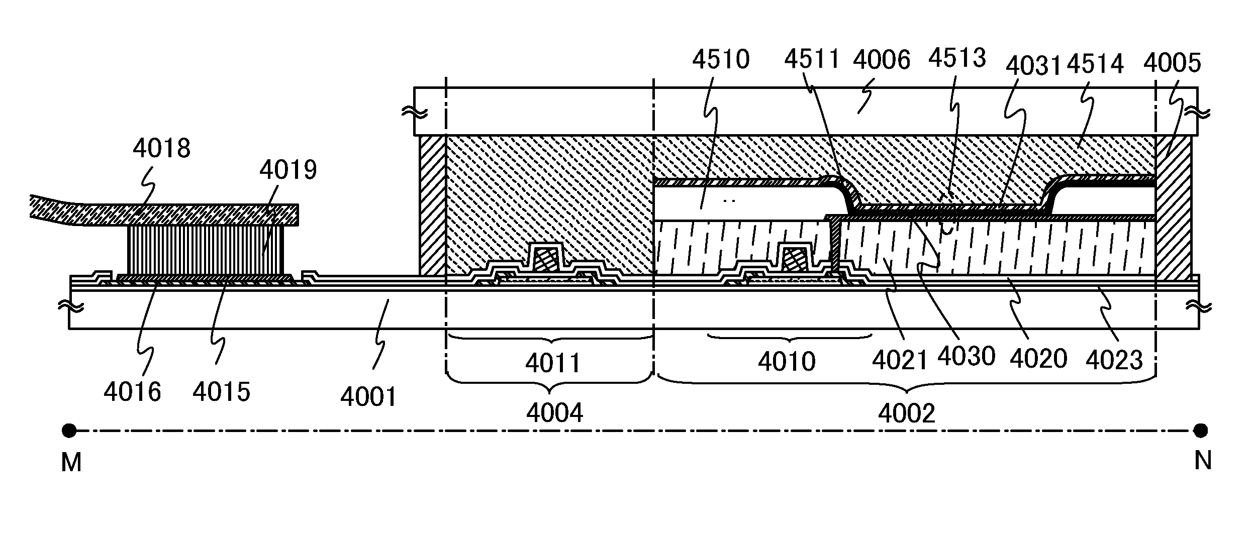
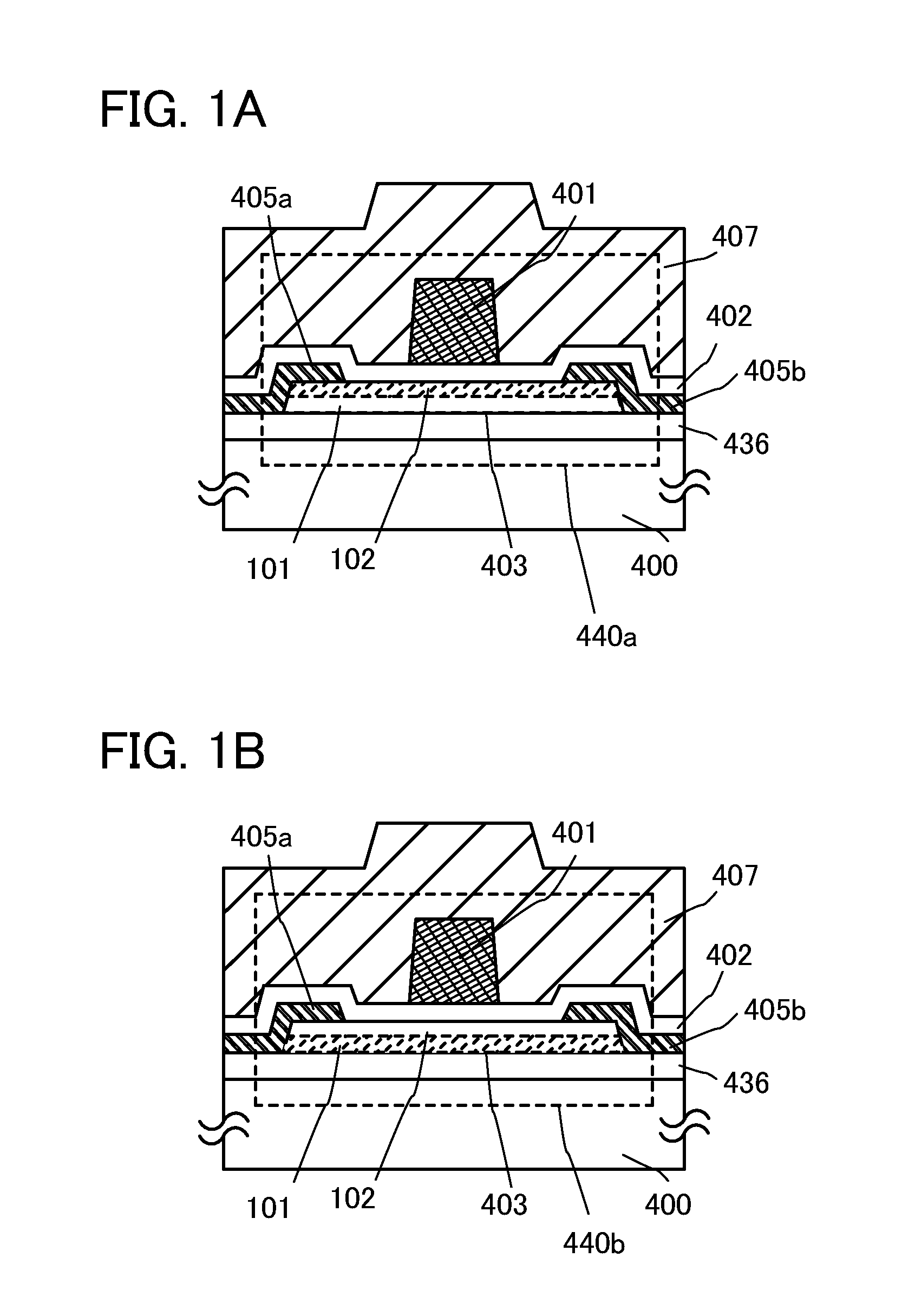
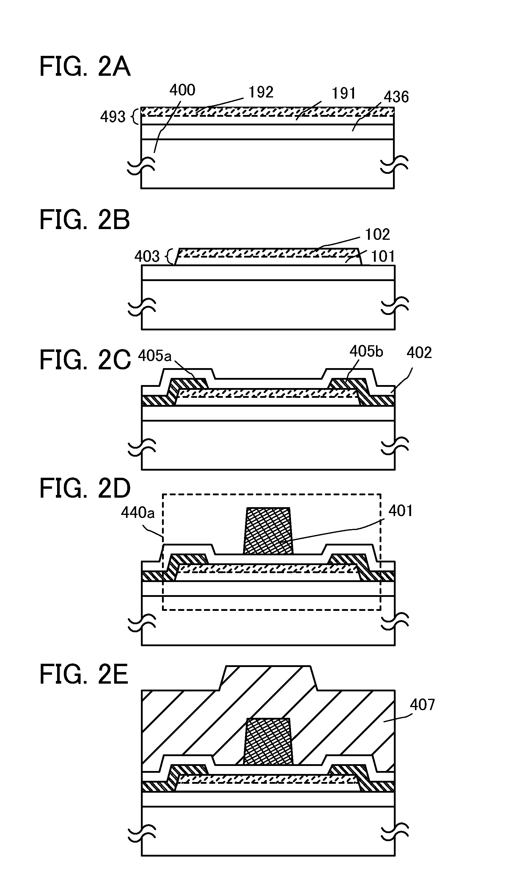
[0058]In this embodiment, modes of semiconductor devices and a method for manufacturing the semiconductor device are described with reference to FIGS. 1A and 1B, FIGS. 2A to 2E, and FIGS. 3A to 3C. In this embodiment, a transistor including an oxide semiconductor film is described as an example of the semiconductor device.

[0059]The transistor may have a single-gate structure in which one channel formation region is formed, a double-gate structure in which two channel formation regions are formed, or a triple-gate structure in which three channel formation regions are formed. Alternatively, the transistor may have a dual-gate structure including two gate electrode layers positioned above and below a channel formation region with a gate insulating film provided therebetween.

[0060]A transistor 440a in FIG. 1A and a transistor 440b in FIG. 1B are examples of planar type transistors having a top-gate structure.

[0061]As illustrated in FIGS. 1A and 1B, the transistors 440a and 440b each in...

embodiment 2

[0177]In this embodiment, another embodiment of a semiconductor device and a method for manufacturing the semiconductor device are described with reference to FIGS. 5A to 5C. The same portions as those in the above embodiment or the portions having functions similar to those in the above embodiment can be formed in manners similar to those of the above embodiment. The same steps as those in the above embodiment and steps similar to those in the above embodiment can be conducted in manners similar to those of the above embodiment. Therefore, the descriptions thereof are not repeated in this embodiment.

[0178]This embodiment shows an example of a method for manufacturing a transistor according to one embodiment of the present invention, oxygen (which contains at least any of an oxygen radical, an oxygen atom, and an oxygen ion) is introduced into an oxide semiconductor stack which has been dehydrated or dehydrogenated to supply oxygen to the film.

[0179]The dehydration or dehydrogenatio...

embodiment 3

[0199]In this embodiment, another embodiment of a semiconductor device and a method for manufacturing the semiconductor device are described with reference to FIGS. 6A to 6C. The same portions as those in the above embodiments or the portions having functions similar to those in the above embodiments can be formed in manners similar to those of the above embodiments. The same steps as those in the above embodiments and steps similar to those in the above embodiments can be conducted in manners similar to those of the above embodiments. Therefore, the descriptions thereof are not repeated in this embodiment.

[0200]This embodiment describes, as an example, the case where a low resistance region is formed in the oxide semiconductor stack in the method for manufacturing the semiconductor device according to one embodiment of the disclosed invention. The low resistance region can be formed by introduction of an impurity (also referred to as dopant) changing the conductivity into the oxide...


PUM


Abstract

A transistor including an oxide semiconductor layer and having electric characteristics required depending on an intended use, and a semiconductor device including the transistor are provided. In a transistor in which a semiconductor layer, a source electrode layer and a drain electrode layer, a gate insulating film, and a gate electrode layer are stacked in this order over an oxide insulating film, an oxide semiconductor stack composed of at least two oxide semiconductor layers having different energy gaps is used as the semiconductor layer. Oxygen and/or a dopant may be introduced into the oxide semiconductor stack.

Description

BACKGROUND OF THE INVENTION[0001]1. Field of the Invention[0002]The present invention relates to a semiconductor device and a method for manufacturing the semiconductor device.[0003]In this specification, a semiconductor device means any device which can function by utilizing semiconductor characteristics, and an electro-optical device, a semiconductor circuit, and an electronic device are all included in the category of the semiconductor device.[0004]2. Description of the Related Art[0005]Attention has been focused on a technique for forming a transistor using a semiconductor thin film (also referred to as a thin film transistor (TFT)). The transistor is applied to a wide range of electronic devices such as an integrated circuit (IC) or an image display device (display device). A silicon-based semiconductor material is widely known as a material for a semiconductor thin film applicable to a transistor. As another material, an oxide semiconductor has been attracting attention.[0006]...

Claims


Application Information

Patent Timeline
Patent Type & Authority Applications(United States)
IPC IPC(8): H01L29/786H01L21/336
CPCH01L29/78618H01L29/78696H01L29/7869
Inventor YAMAZAKI, SHUNPEIHONDA, TATSUYA
Owner SEMICON ENERGY LAB CO LTD
Why Eureka
Try Eureka