Encapsulating sheet and optical semiconductor element device

a technology of optical semiconductor elements and encapsulating sheets, which is applied in the direction of radiation control devices, synthetic resin layered products, transportation and packaging, etc., can solve the problems of affecting the appearance of semiconductor light emitting devices, bleed of residual monomer (an unreacted liquid resin) in resin encapsulating materials, etc., to improve the appearance of optical semiconductor element devices, and suppress the bleeding of residual monomer

Inactive Publication Date: 2012-12-20
NITTO DENKO CORP
View PDF1 Cites 23 Cited by
  • Summary
  • Abstract
  • Description
  • Claims
  • Application Information

AI Technical Summary

Benefits of technology

[0009]However, in the semiconductor light emitting device described in Japanese Unexamined Patent Publication No. 2001-358368, there may be a case where the temperature of the resin encapsulating material is increased by heat generation of the LED and the phosphor cover along with the light emission, so that a bleeding of a residual monomer (an unreacted liquid resin) in the resin encapsulating material occurs. In this way, there is a disadvantage of damaging the appearance of the semiconductor light emitting device.
[0010]It is an object of the present invention to provide an encapsulating sheet that is capable of suppressing a bleeding in an encapsulating resin layer and improving the appearance of an optical semiconductor element device, and the optical semiconductor element device that is encapsulated by the encapsulating sheet.
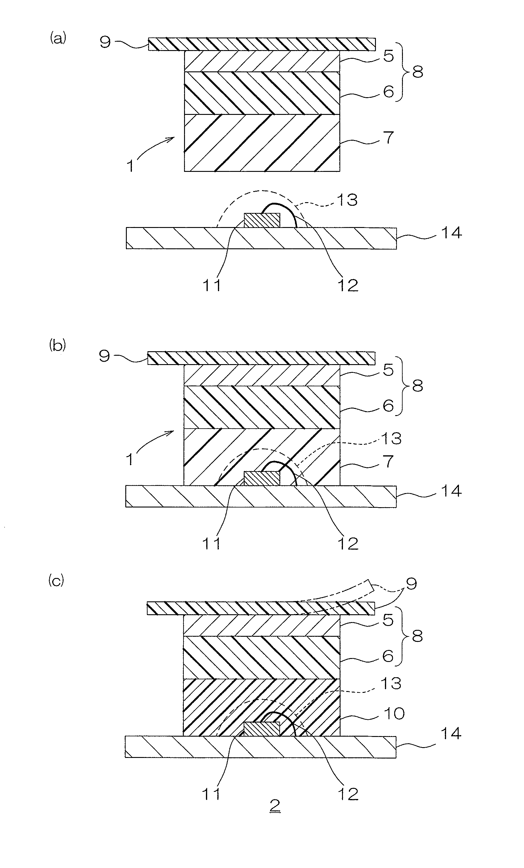
[0017]Therefore, in the optical semiconductor element device in which the optical semiconductor element is encapsulated by the encapsulating sheet of the present invention, even when the optical semiconductor element and the phosphor layer generate heat along with the light emission, the bleeding of the residual monomer (the unreacted liquid resin) in the encapsulating resin layer can be suppressed by the barrier layer. As a result, it is possible to improve the appearance of the optical semiconductor element device.
[0018]Accordingly, the encapsulating sheet of the present invention can suppress the bleeding of the residual monomer (the unreacted liquid resin) in the encapsulating resin layer and improve the appearance of the optical semiconductor element device.

Problems solved by technology

However, in the semiconductor light emitting device described in Japanese Unexamined Patent Publication No. 2001-358368, there may be a case where the temperature of the resin encapsulating material is increased by heat generation of the LED and the phosphor cover along with the light emission, so that a bleeding of a residual monomer (an unreacted liquid resin) in the resin encapsulating material occurs.
In this way, there is a disadvantage of damaging the appearance of the semiconductor light emitting device.

Method used


Image

  • Encapsulating sheet and optical semiconductor element device
  • Encapsulating sheet and optical semiconductor element device
  • Encapsulating sheet and optical semiconductor element device

Examples


prepared example 1

[0373]26 g of YAG:Ce was mixed to 74 g of a mixed solution (mixing ratio (A / B)=1 / 1) in which A liquid (a polysiloxane containing an ethylenically unsaturated hydrocarbon group) and B liquid (an organohydrogensiloxane) of an addition reaction curable type silicone resin composition (LR7665, manufactured by WACKER ASAHIKASEI SILICONE CO., LTD.) were mixed to be stirred for 1 hour. After the stirring, the obtained mixture was subjected to a defoaming process under reduced pressure with a vacuum dryer at room temperature for 30 minutes or more.

[0374]In this way, a resin composition containing a phosphor was prepared (a phosphor concentration of 26 mass %).

Preparation of Encapsulating Resin Composition

prepared example 2

Preparation of Encapsulating Resin Composition A

[0375]15.76 g (0.106 moles) of vinyltrimethoxysilane (an ethylenic silicon compound) and 2.80 g (0.0118 moles) of (3-glycidoxypropyl)trimethoxysilane (a silicon compound containing an epoxy group) were blended into 2031 g (0.177 moles) of polydimethylsiloxane containing silanol groups at both ends (polysiloxane containing silanol groups at both ends, in formula (1), all of R1s are methyl groups, the average of “n” is 155, a number average molecular weight of 11500, a silanol group equivalent of 0.174 mmol / g), which was heated at 40° C., and the obtained mixture was stirred and mixed.

[0376]The molar ratio (the mole number of the SiOH group / the total mole number of the SiOCH3 group) of the SiOH group in the polydimethylsiloxane containing silanol groups at both ends to the SiOCH3 group in the vinyltrimethoxysilane and (3-glycidoxypropyl)trimethoxysilane was 1 / 1.

[0377]After the stirring and mixing, 0.97 mL (0.766 g, a catalyst content: 0....

prepared example 3

Preparation of Encapsulating Resin Composition B

[0383]600 g (0.200 moles) of a dual-end silanol type silicone oil (trade name: KF-9701, manufactured by Shin-Etsu Chemical Co., Ltd., an average molecular weight of 3000) and 8.22 g (40.2 moles) of aluminum isopropoxide were stirred and mixed at room temperature (25° C.) for 24 hours, so that a mixture was prepared.

[0384]Next, the obtained mixture was centrifuged to remove insoluble substances and the resulting mixture was concentrated under reduced pressure at 50° C. for 2 hours, so that a polyaluminosiloxane oil was obtained.

[0385]Next, 10 parts by mass of a methacrylic silane coupling agent (trade name: KBM-503, manufactured by Shin-Etsu Chemical Co., Ltd.) was added to 100 parts by mass of the obtained polyaluminosiloxane oil to be stirred under reduced pressure at 80° C. for 10 minutes.

[0386]Next, 10 g of a filler A (silicon dioxide, trade name: FB-3SDC, manufactured by DENKI KAGAKU KOGYO KABUSHIKI KAISHA., an average particle siz...


PUM

PropertyMeasurementUnit
thicknessaaaaaaaaaa
elastic modulusaaaaaaaaaa
energyaaaaaaaaaa

Abstract

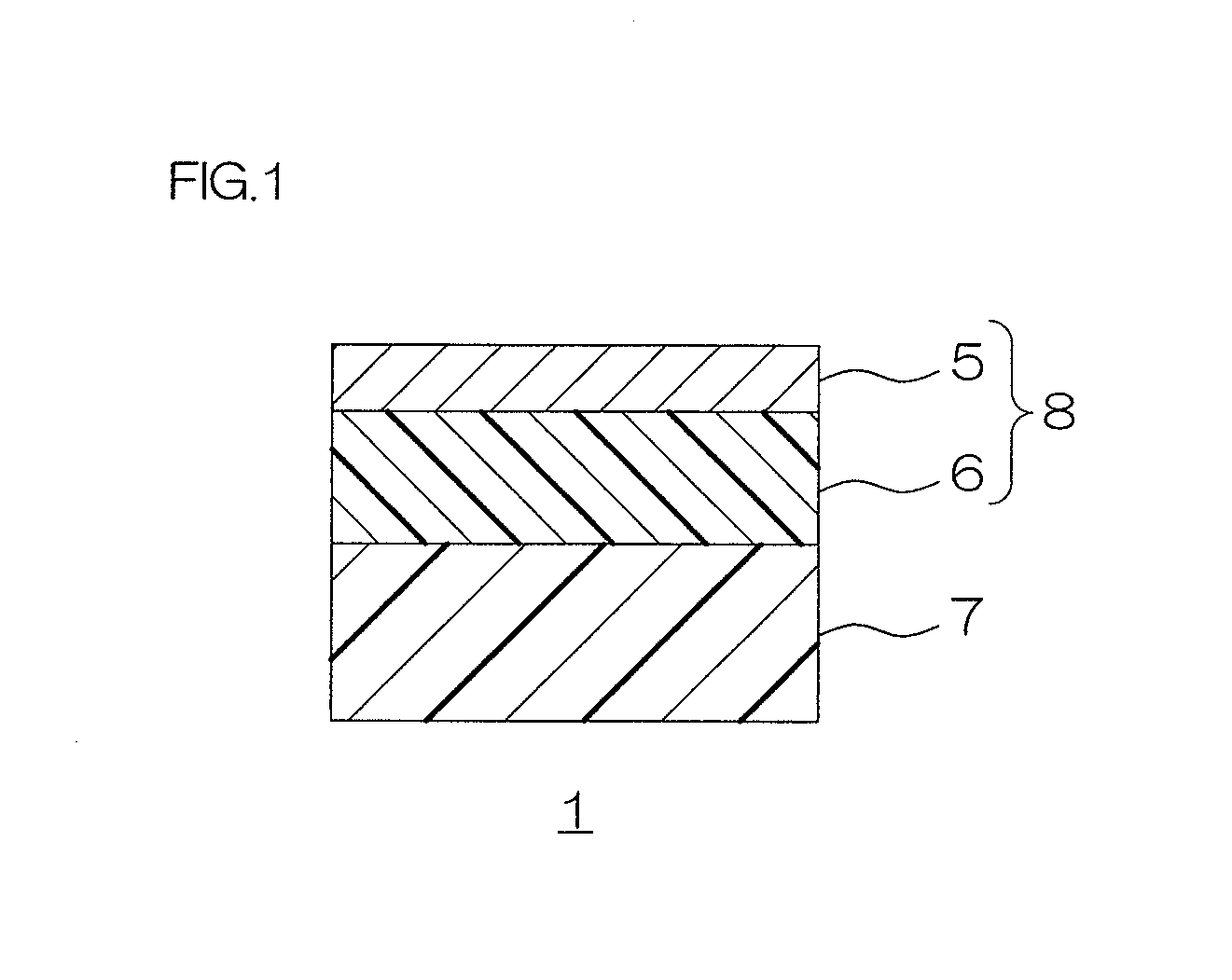
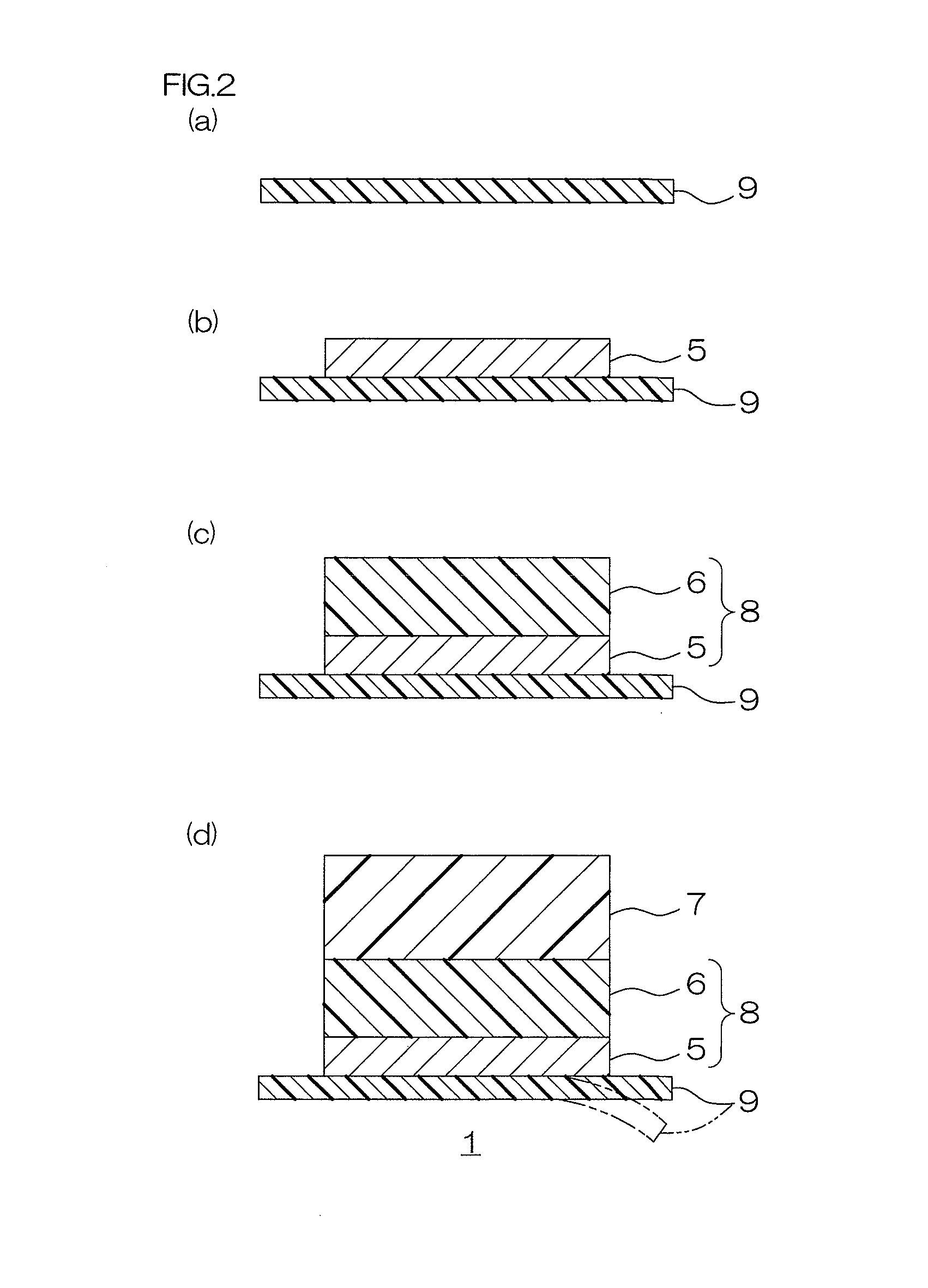
An encapsulating sheet includes an encapsulating resin layer and a wavelength conversion layer laminated on the encapsulating resin layer. The wavelength conversion layer is formed by laminating a barrier layer formed of a light transmissive resin composition and having a thickness of 200 μm to 1000 μm, and a phosphor layer containing a phosphor.

Description

CROSS-REFERENCE TO RELATED APPLICATION[0001]The present application claims priority from Japanese Patent Applications No. 2011-132275 filed on Jun. 14, 2011 and No. 2011-228921 filed on Oct. 18, 2011, the contents of which are hereby incorporated by reference into this application.BACKGROUND OF THE INVENTION[0002]1. Field of the Invention[0003]The present invention relates to an encapsulating sheet and an optical semiconductor element device, to be specific, to an optical semiconductor element device used for an optical application and an encapsulating sheet used therein.[0004]2. Description of Related Art[0005]Conventionally, as a light emitting device that is capable of emitting high-energy light, a white light emitting device has been known.[0006]In the white light emitting device, for example, blue light is emitted by an optical semiconductor and a part of the emitted blue light is converted into yellow light by a phosphor layer containing a phosphor, so that white light is emit...

Claims


Application Information

Patent Timeline
Patent Type & Authority Applications(United States)
IPC IPC(8): H01L33/50B32B27/08
CPCB29C43/18H01L33/505H01L33/507H01L33/54H01L33/56Y10T428/269H01L2933/005H01L2224/48091H01L2933/0041H01L2924/00014H01L33/50H01L33/52
Inventor MATSUDA, HIROKAZUKONDO, TAKASHIKONO, HIROKI
Owner NITTO DENKO CORP
Why Eureka
Try Eureka