Micro-pattern transferring stamper

a stamper and micro-pattern technology, applied in the field of micro-pattern transfer stampers, can solve the problems of reducing throughput, taking a long time to complete the drawing of patterns, and affecting the transfer accuracy of patterns, so as to achieve the effect of not reducing the transfer precision of patterns

Inactive Publication Date: 2012-12-20
HITACHI HIGH-TECH CORP
View PDF2 Cites 26 Cited by
  • Summary
  • Abstract
  • Description
  • Claims
  • Application Information

AI Technical Summary

Benefits of technology

[0014]According to the present invention, it becomes possible to provide the micro-pattern transferring stamper that is a soft stamper having

Problems solved by technology

However, miniaturization of such patterns becomes advanced and when a required process dimension becomes small to the wavelength of light or so used for an exposure, it becomes difficult for the photolithography technologies to cope with such miniaturization.
The larger then number of the patterns to be drawn is, the more the exposure (lithography) time increases, and thus it takes a time to complete the drawing of patterns.

Method used


Image

  • Micro-pattern transferring stamper
  • Micro-pattern transferring stamper
  • Micro-pattern transferring stamper

Examples


examples

[0095]Next, the present invention will be explained in more detail with reference to the examples. Terms “pts” and “%” used in the following explanation are all mass standards except that there is a special indication.

first example

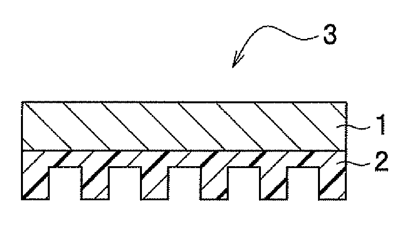
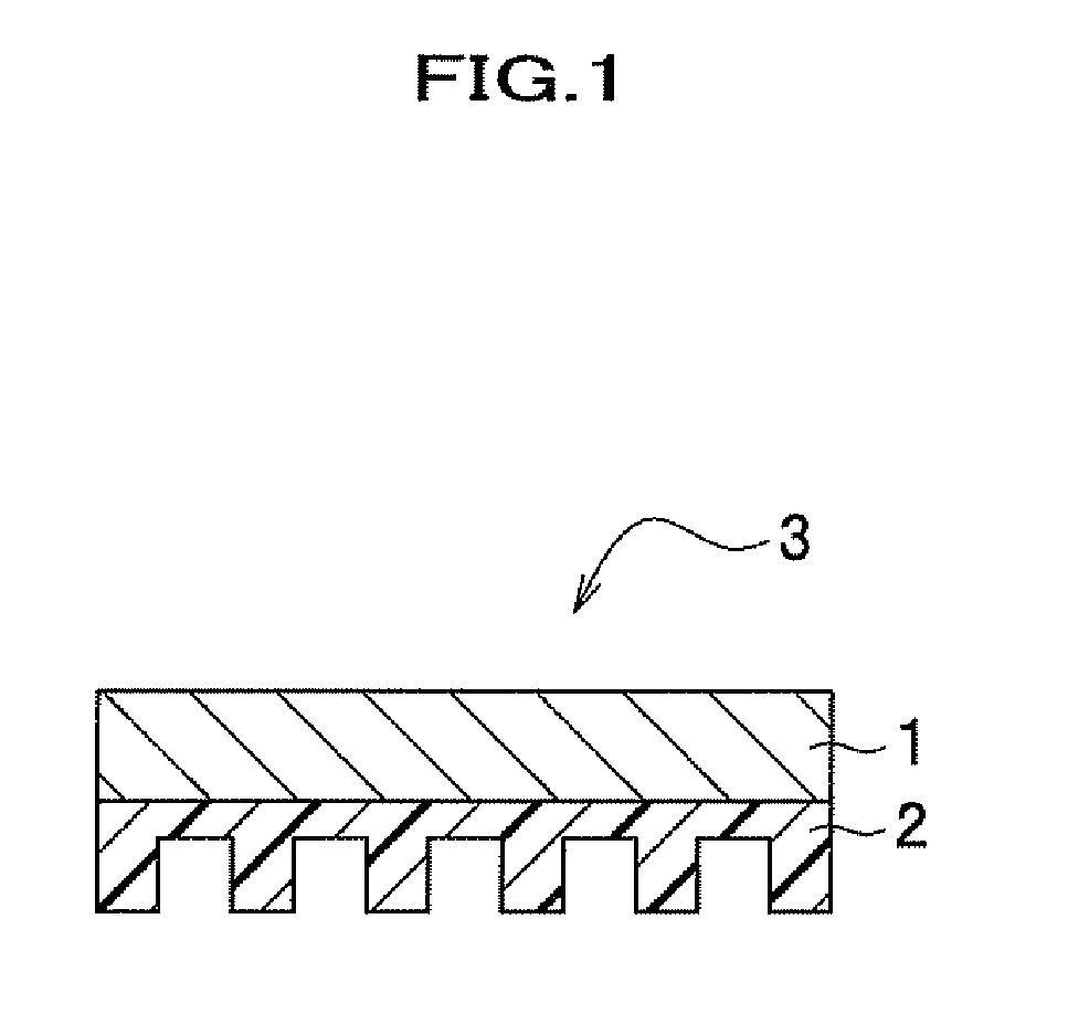
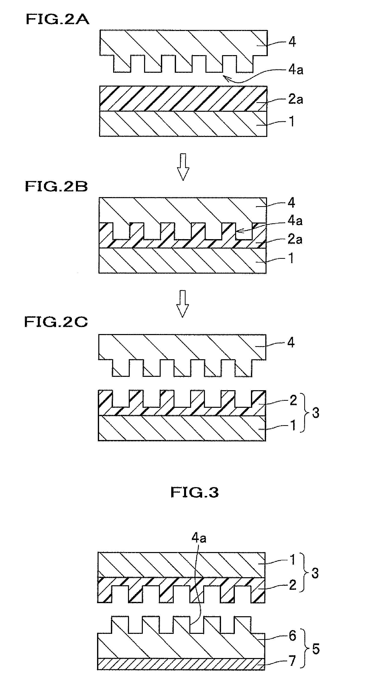
[0096]According to this example, the micro-pattern transferring stamper 3 was produced through the processes shown in FIGS. 2A to 2C.

[0097]2a>

[0098]First of all, as shown in following table 1, 0.7 pts of silsesquioxane derivative OX-SQ SI-20 (made by TOA GOSEI Corporation, indicated as SQ(a) in table 1. The same is true of the following explanation) having a plurality of oxetanyl groups, 0.3 pts of 3-ethyl-3-{[3-ethyloxetane-3-yl]methoxymethyl}oxetane (made by TOA GOSEI Corporation, indicated as monomer element (a) in table 1. The same is true of the following explanation) that was bifunctional oxetane as the monomer element, and 0.06 pts of ADEKA OPTOMER-SP-172 (made by ASAHI DENKA Corporation, simply indicated as “polymerization initiator” in table 1. The same is true of the following explanation) as a cationic polymerization initiator were blended to prepare a photo-curable resin composition 2a for forming a microstructure layer 3.

[0099]The functional group equivalent amount [...

second example

[0109]In this example, the micro-pattern transferring stamper 3 having the microstructure layer 2 was produced through the same method as that of the first example. In this case, the resin composition 2a was prepared through the same way as that of the first example except that the silsesquioxane derivative OX-SQ SI-20 (made by TOA GOSEI Corporation) indicated as SQ (a) in table 1 was set to be 0.9 pts and instead of the monomer element (a) in table 1, 0.1 pts of 1,4-bis(2,3-epoxypropyl)perfluorobutane (made by DAIKIN Industries Corporation, indicated as monomer element (b) in table 1. The same is true of the following explanation) that was diepoxy having a perfluoro skeleton was used, and the micro-pattern transferring stamper 3 was produced using those materials. Table 1 shows a functional group equivalent amount [g / eq] of the resin composition 2a, and an elastic modulus [Pa], a curing shrinkage percentage [%], and an inorganic fraction [mass %] of the microstructure layer 2.

[0110...


PUM

PropertyMeasurementUnit
Percent by massaaaaaaaaaa
Shrinkageaaaaaaaaaa

Abstract

A micro-pattern transferring stamper includes a supporting base material and a microstructure layer formed on the supporting base material, the microstructure layer is a polymer of a resin composition that mainly contains a silsesquioxane derivative containing a plurality of polymerizable functional groups, and one or plural kinds of monomer elements containing a plurality of polymerizable functional groups.

Description

TECHNICAL FIELD[0001]The present invention relates to a micro-pattern transferring stamper that is pushed against a transfer target to form a microstructure (a fine pattern) on a surface of the transfer target.BACKGROUND ART[0002]Conventionally, photolithography technologies are used as the technologies to form fine patterns that are required for a semiconductor device, etc. However, miniaturization of such patterns becomes advanced and when a required process dimension becomes small to the wavelength of light or so used for an exposure, it becomes difficult for the photolithography technologies to cope with such miniaturization. Hence, instead of the photolithography technologies, electron beam lithography devices that are a kind of charged particle beam devices become nowadays popular.[0003]The pattern formation using such electron beams applies a technique of directly drawing a mask pattern unlike one-shot exposure techniques using light sources, such as i rays and excimer laser,...

Claims


Application Information

Patent Timeline
IPC IPC(8): B29C59/16B29C59/02
CPCB82Y10/00B82Y40/00G03F7/0002G11B5/855G03F7/0046G03F7/038G03F7/0757
Inventor ISHII, SATOSHIOGINO, MASAHIKOSHIZAWA, NORITAKEMORI, KYOICHIMIYAUCHI, AKIHIRO
Owner HITACHI HIGH-TECH CORP
Why Eureka
Try Eureka