Solar battery
- Summary
- Abstract
- Description
- Claims
- Application Information
AI Technical Summary
Benefits of technology
Problems solved by technology
Method used
Image

Examples
first embodiment
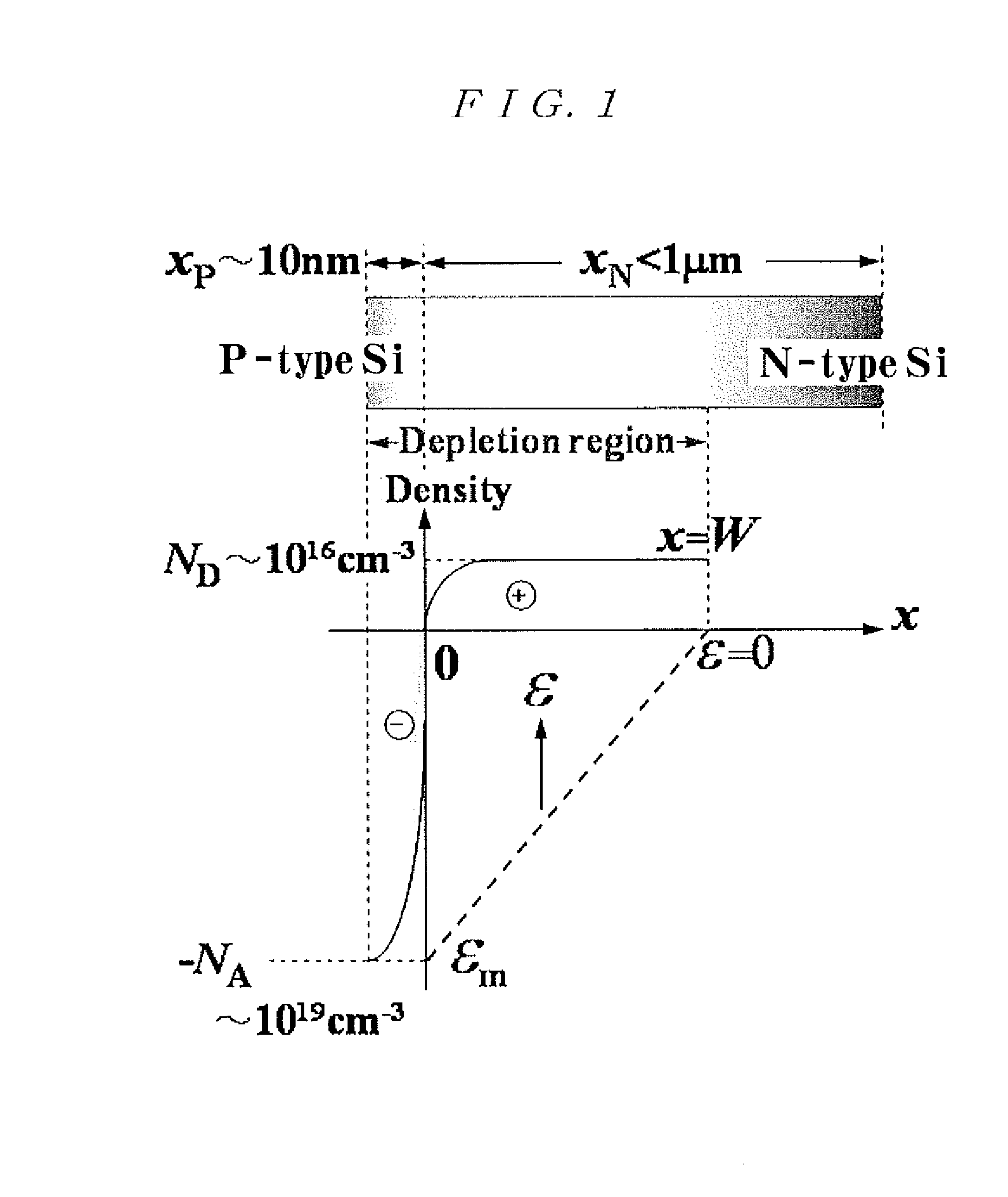
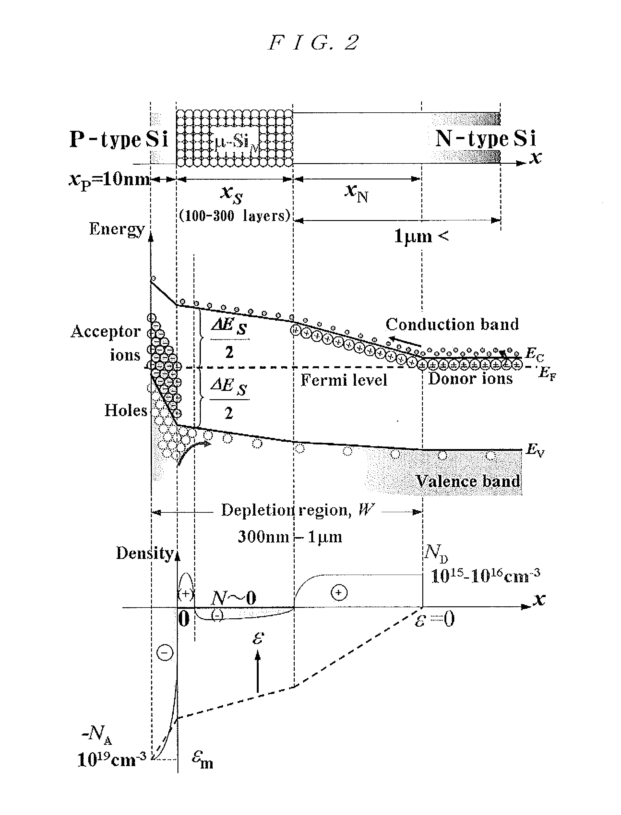
[0056]A silicon cluster solar battery device according to the present invention will be explained. The first embodiment describes a design guideline necessary for fabricating a practical solar battery utilizing a μ-SiN silicon cluster refined to 2 nm to 2.5 nm in particle diameter, by the use of the silicon cluster technology introduced in the present invention. The present first embodiment solves the above-identified technical problems 2 and 3.
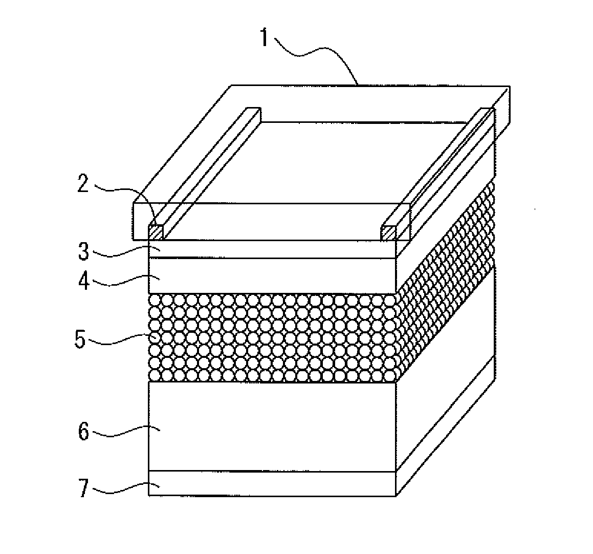
[0057]The first embodiment is the basic structure of the present invention which is related to all silicon μ-SiN-N junction where a refined silicon cluster is inserted between the P-N junction on the basis of the simplest P-N junction. This is a basic solar battery structure of the present invention. FIG. 4 is a view showing a device structure of the silicon cluster solar battery. The first embodiment will be described referring to FIG. 4. As shown in FIG. 4, the device according to the first embodiment comprises a glass substrate 1; a lead-o...
second embodiment
[0072]The second embodiment according to the present invention further provides a passivation film in addition to the elements in the first embodiment. The second embodiment will be explained referring to FIG. 7. FIG. 7 is a view showing a device structure according to the second embodiment. As shown in FIG. 4, the device according to the second embodiment includes a glass substrate 21; a lead-out electrode 22; a transparent electrode 23; a P-type fine crystal silicon 24; a passivation film 25; a quantum dot 26 of the silicon cluster (μ-SiN); N-type amorphous silicon or N-type fine crystal silicon 27, and an electrode 28. Typically, as a device structure according to the second embodiment, the Ag lead-out electrode 22 is firstly embedded in the glass substrate 21 so as to expose thereon its surface of the electrode, and the transparent electrode 23, such as an ITO is deposited thereon. Then, P-type fine crystal silicon (μ-Si, thickness 10 nm) 24, the passivation film (graphite singl...
PUM
| Property | Measurement | Unit |
|---|---|---|
| Thickness | aaaaa | aaaaa |
| Nanoscale particle size | aaaaa | aaaaa |
| Nanoscale particle size | aaaaa | aaaaa |
Abstract
Description
Claims
Application Information