
Semiconductor integrated circuit device

a technology of integrated circuits and semiconductors, applied in electronic switching, capacitors, pulse techniques, etc., can solve the problem of increasing harmonic distortion, and achieve the effect of reducing the manufacturing cost of antenna switches, enhancing the performance of antenna switches, and reducing second-order harmonic distortion

Inactive Publication Date: 2013-01-03
RENESAS ELECTRONICS CORP
View PDF3 Cites 5 Cited by
  • Summary
  • Abstract
  • Description
  • Claims
  • Application Information

AI Technical Summary

Benefits of technology

The invention aims to use SOI MOSFETs for switching of an antenna switch while reducing harmonic distortion. This technology can significantly reduce second- and third-order harmonic distortion in the antenna switch, which would otherwise cause performance issues. By doing this, the manufacturing cost of the antenna switch can be reduced while improving its performance.

Problems solved by technology

When SOI MOSFETs are used for the transistors for switching in an antenna switch circuit, harmonic distortion becomes larger than in cases where compound semiconductor FETs are used for this purpose.

Method used


Image

  • Semiconductor integrated circuit device
  • Semiconductor integrated circuit device
  • Semiconductor integrated circuit device

Examples


first embodiment

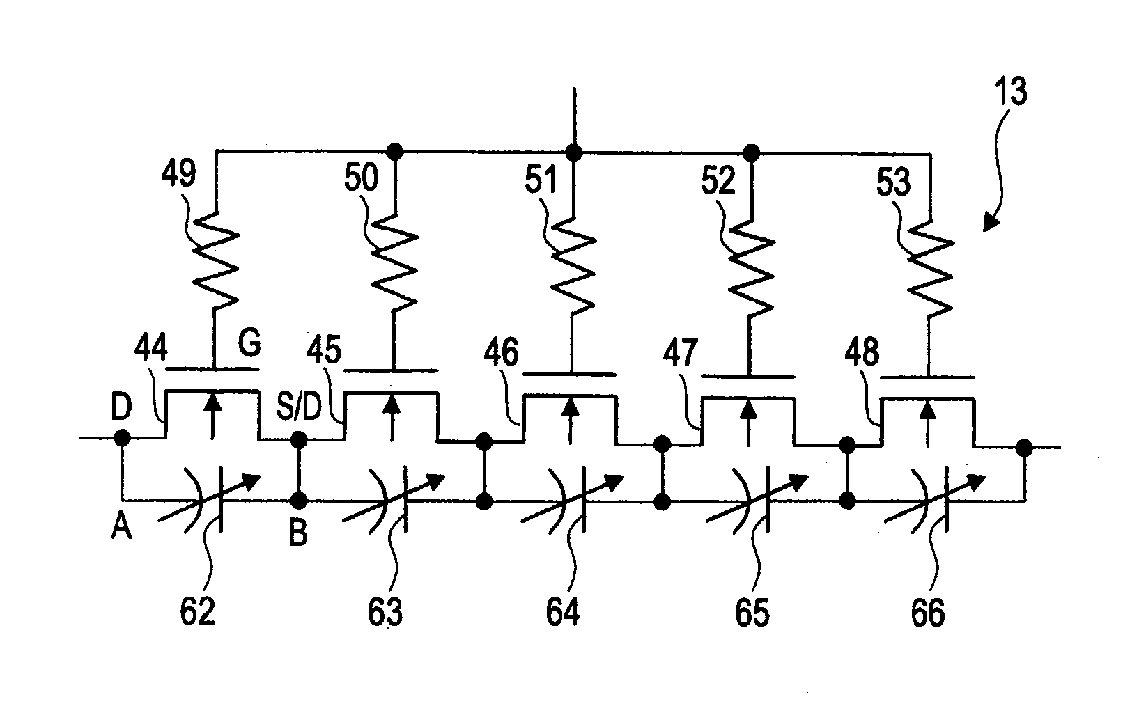
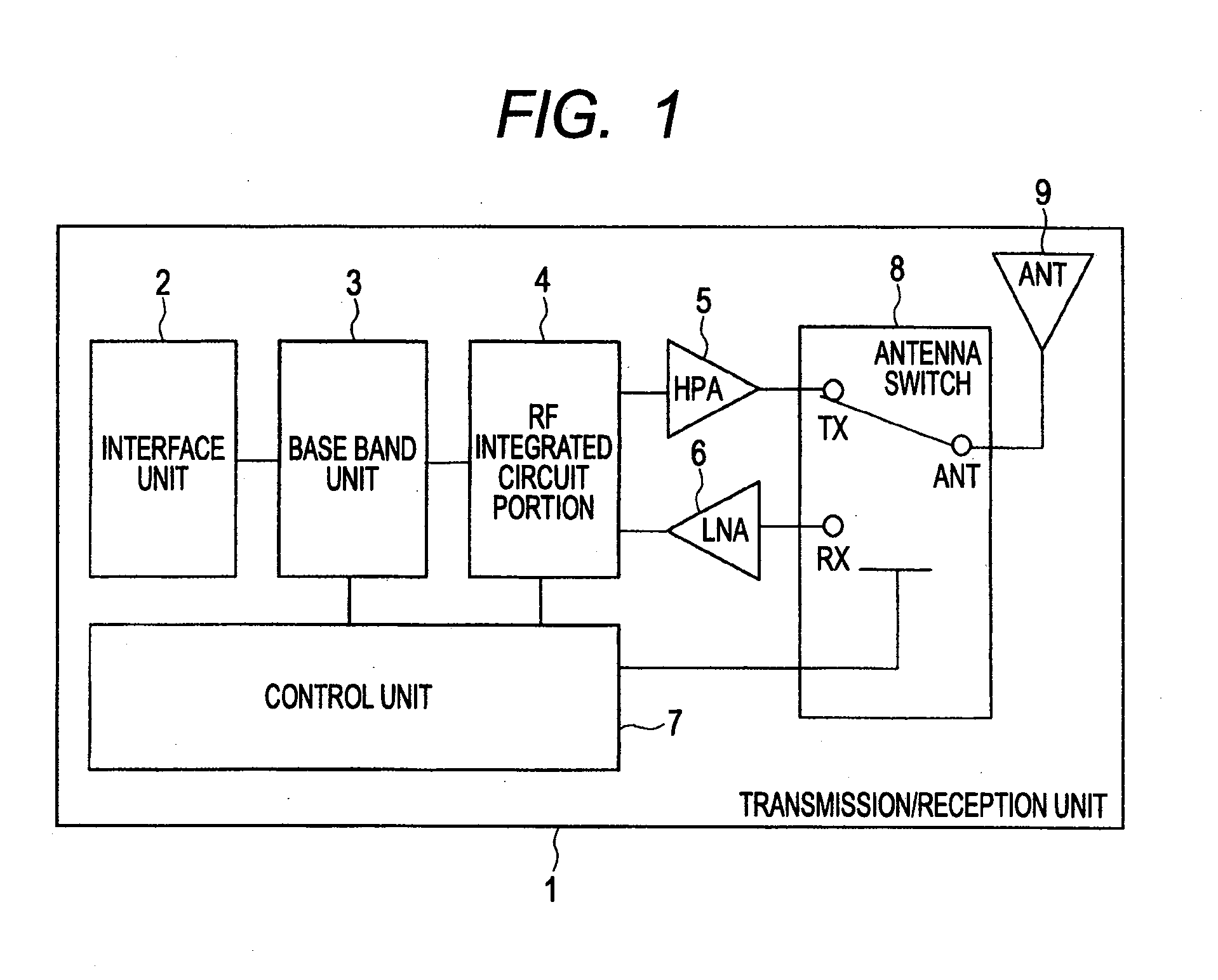
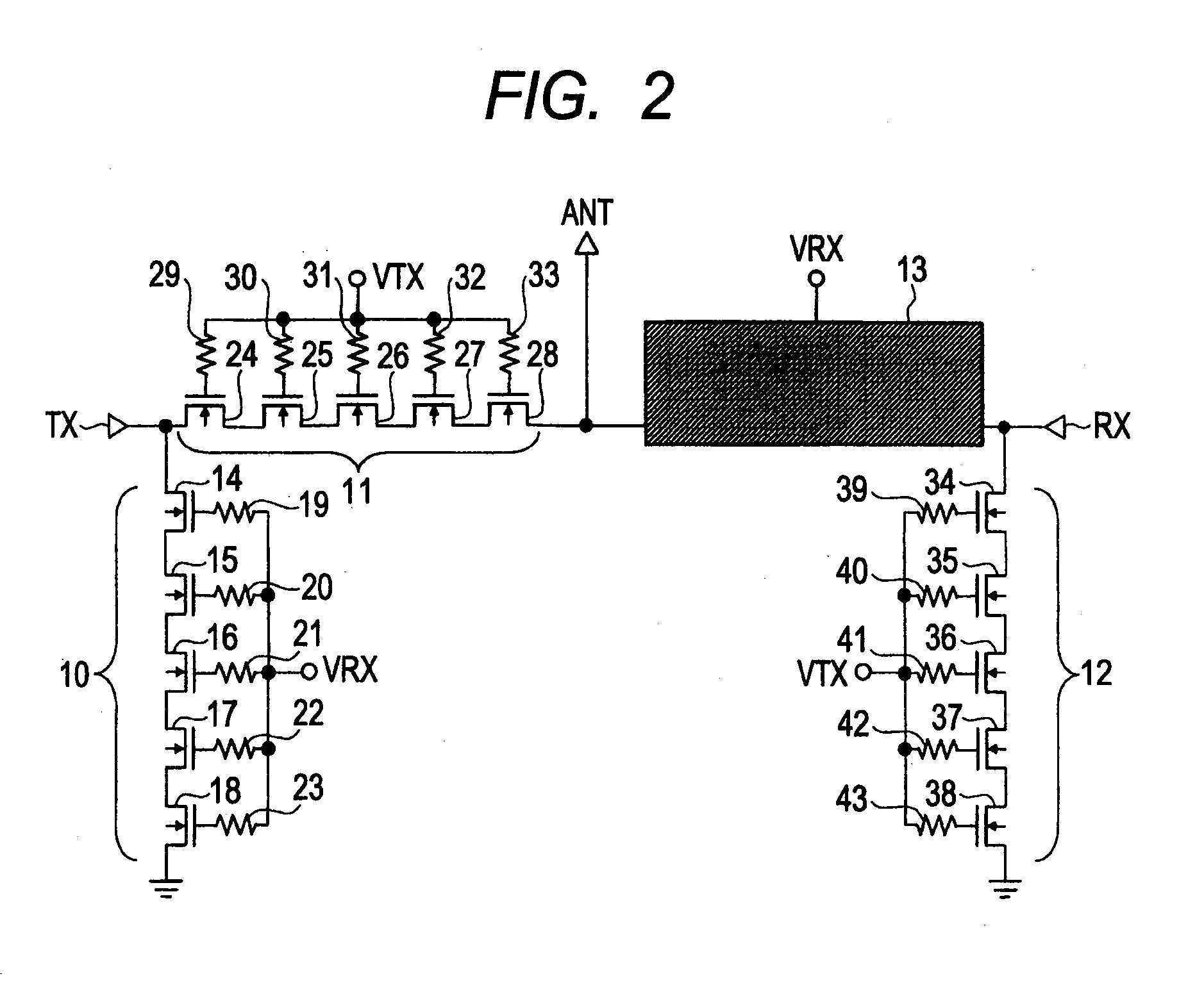
[0079]FIG. 1 is a block diagram illustrating an example of the configuration of a transmission / reception unit provided in a cellular phone in the first embodiment of the invention; FIG. 2 is a circuit diagram illustrating an example of an antenna switch provided in the transmission / reception unit in FIG. 1; FIG. 3 is a circuit diagram illustrating an example of a through MOSFET group of reception branch comprising the antenna switch in FIG. 2; FIG. 4 is a schematic diagram illustrating an example of the layout in the through MOSFET group of reception branch in FIG. 3; FIG. 5 is an explanatory drawing illustrating the voltage dependence of the substrate capacitance of SOI MOSFET; and FIG. 6 is an explanatory drawing illustrating the voltage dependence of the source-drain parasitic capacitance of SOI MOSFET.

[0080]In the first embodiment, the transmission / reception unit 1 used in, for example, a cellular phone is provided with the following members as illustrated in FIG. 1: an interfac...

second embodiment

[0125]FIG. 7 is a circuit diagram illustrating an example of a through MOSFET group of reception branch in the second embodiment of the invention; FIG. 8 is an explanatory drawing illustrating an example of the layout in a capacitance element for reducing second-order harmonic distortion provided in the through MOSFET group of reception branch in FIG. 7; FIG. 9 is an explanatory drawing illustrating the voltage dependence of the capacitance value of the capacitance element in FIG. 8; FIG. 10 is an explanatory drawing illustrating an example of a section taken along line a-b of FIG. 8; FIG. 11 is a symbol diagram representing the capacitance element in FIG. 8; and FIG. 12 is an explanatory drawing illustrating an example of the plane layout of the through MOSFET group of reception branch in FIG. 7.

[0126]With respect to the second embodiment, description will be given to a technology for adding the following capacitance element to between the source and drain of a transistor of the an...

third embodiment

[0153]FIG. 13 is a circuit diagram illustrating an example of a through MOSFET group of reception branch in the third embodiment of the invention; and FIG. 14 is an explanatory drawing illustrating an example of the layout in a capacitance element for reducing second-order harmonic distortion provided in the through MOSFET group of reception branch in FIG. 13.

[0154]In the third embodiment, capacitance elements differing in voltage dependence depending on the polarity of voltage are inserted. The capacitance elements are inserted into between the respective sources and ground or between the respective drains and ground of the transistors 44 to 48 in the through MOSFET group of reception branch 13. The voltage dependence of each of these capacitance elements is set so as to compensate the influence of the voltage dependence of substrate capacitance asymmetric with respect to the polarity of voltage on the circuit characteristics.

[0155]The antenna switch 8 is comprised as in FIG. 2 in ...


PUM


Abstract

SOI MOSFETs are used for the transistors for switching of an antenna switch and yet harmonic distortion is significantly reduced. Capacitance elements are respectively added to either the respective drains or gates of the transistors comprising the through MOSFET group of reception branch of the antenna switch. This makes the voltage amplitude between source and gate and that between drain and gate different from each other. As a result, the voltage dependence of source-drain parasitic capacitance becomes asymmetric with respect to the polarity of voltage. This asymmetry property produces signal distortion having similar asymmetry property. Therefore, the following can be implemented by setting it so that it has the same amplitude as that of second-harmonic waves arising from the voltage dependence of substrate capacitance and a phase opposite to that of the same: second-order harmonic distortion can be canceled out and thus second-order harmonic distortion can be reduced.

Description

CROSS-REFERENCE TO RELATED APPLICATIONS[0001]This application is a divisional of U.S. patent application Ser. No. 12 / 813,852, filed Jun. 11, 2010, which claims priority to Japanese Patent Application No. 2009-158995 filed on Jul. 3, 2009, the disclosure of which, including the specification, drawings and abstract, is incorporated herein by reference in its entirety.BACKGROUND OF THE INVENTION[0002]The present invention relates to technologies for reducing harmonic distortion in antenna switches used in mobile communication devices or the like and in particular to a technology effectively applicable to the reduction of second-order harmonic distortion and third-order harmonic distortion in an antenna switch configured using SOI MOSFETs (Silicon On Insulator Metal Oxide Semiconductor Field Effect Transistors).[0003]In antenna switches for switching between transmission and reception used in cellular phones or the like, in general, a compound semiconductor FET such as HEMT (High Electr...

Claims


Application Information

Patent Timeline
Patent Type & Authority Applications(United States)
IPC IPC(8): H03K17/56H01L29/92
CPCH01L27/0207H01L27/1203H04B1/48H01L29/94H01L28/86
Inventor KONDO, MASAOGOTO, SATOSHIMORIKAWA, MASATOSHI
Owner RENESAS ELECTRONICS CORP
Learn More