Semiconductor module

a technology of semiconductor modules and modules, applied in the direction of semiconductor devices, semiconductor/solid-state device details, electrical apparatus, etc., can solve the problems of shortening the life of joint parts formed, dlb technique entails higher cost than wire bonding technique, and achieves the effect of low cost manufacturing

Inactive Publication Date: 2013-01-10
MITSUBISHI ELECTRIC CORP
View PDF1 Cites 26 Cited by
  • Summary
  • Abstract
  • Description
  • Claims
  • Application Information

AI Technical Summary

Benefits of technology

[0009]It is an object of the present invention to provide a semiconductor module that can be manufactured at low cost while the reliability of an electrode terminal thereof is maintained.
[0011]In the first semiconductor module of the present invention, the lead frame is solder-joined on the power device chip. This increases a joint area compared to that obtained by wire bonding, thereby providing high reliability of resistance to heat stress to be generated by turning on and off the power device chip. Further, one end of the lead frame is joined on the metal pattern different from the metal pattern on which the power device chip is placed, making it possible to reduce the temperature of the lead frame during the semiconductor module is in operation. Sill further, the lead frame and the external main electrode are joined to each other by wire bonding on the metal pattern at a temperature lower than that around the power device chip. So, even inexpensive wire bonding can maintain reliability at a high level. In addition, formation of the sealing resin by potting does not place many limitations on the shape or dimension of a terminal. This allows the semiconductor module to be applied easily to a product group of a wide variety of types, or to a small group of products.
[0013]In the second semiconductor module of the present invention, provision of the single metal pattern on the insulating plate increases the temperature of a junction between the lead frame and a bonding wire, compared to the case where divided metal patterns are provided. However, provision of the single metal pattern prevents insulation degradation between different electrodes, thereby enhancing insulating strength.
[0015]In the third semiconductor module of the present invention, the lead frame is wire-bonded to the external main electrode above the free-wheeling diode chip. So, the temperature of a junction part thereof is made higher. However, the size of the lead frame can be made closer to the projected areas of the power device chip and the free-wheeling diode chip, allowing size reduction of the semiconductor module. This structure is applied usefully if size reduction is given priority than the life span of a semiconductor module.

Problems solved by technology

However, this technique shortens the life span of a joint part formed by wire bonding due to heat stress generated by turning the power device on and off repeatedly.
So, the maximum junction temperature should be set low if increase of a life span is given higher priority, resulting in the size increase or cost increase of a power module.
While enhancing the reliability of a joint part, the DLB technique entails higher cost than the wire bonding technique.
However, the transfer molding technique involves a large amount of initial investment to prepare a mold, for example, placing limitations on the degree of freedom of a terminal shape or dimensions.
So, applying the transfer molding technique to a product group of a wide variety of types, or to a small group of products causes a problem of cost increase.

Method used


Image

  • Semiconductor module
  • Semiconductor module
  • Semiconductor module

Examples


first preferred embodiment

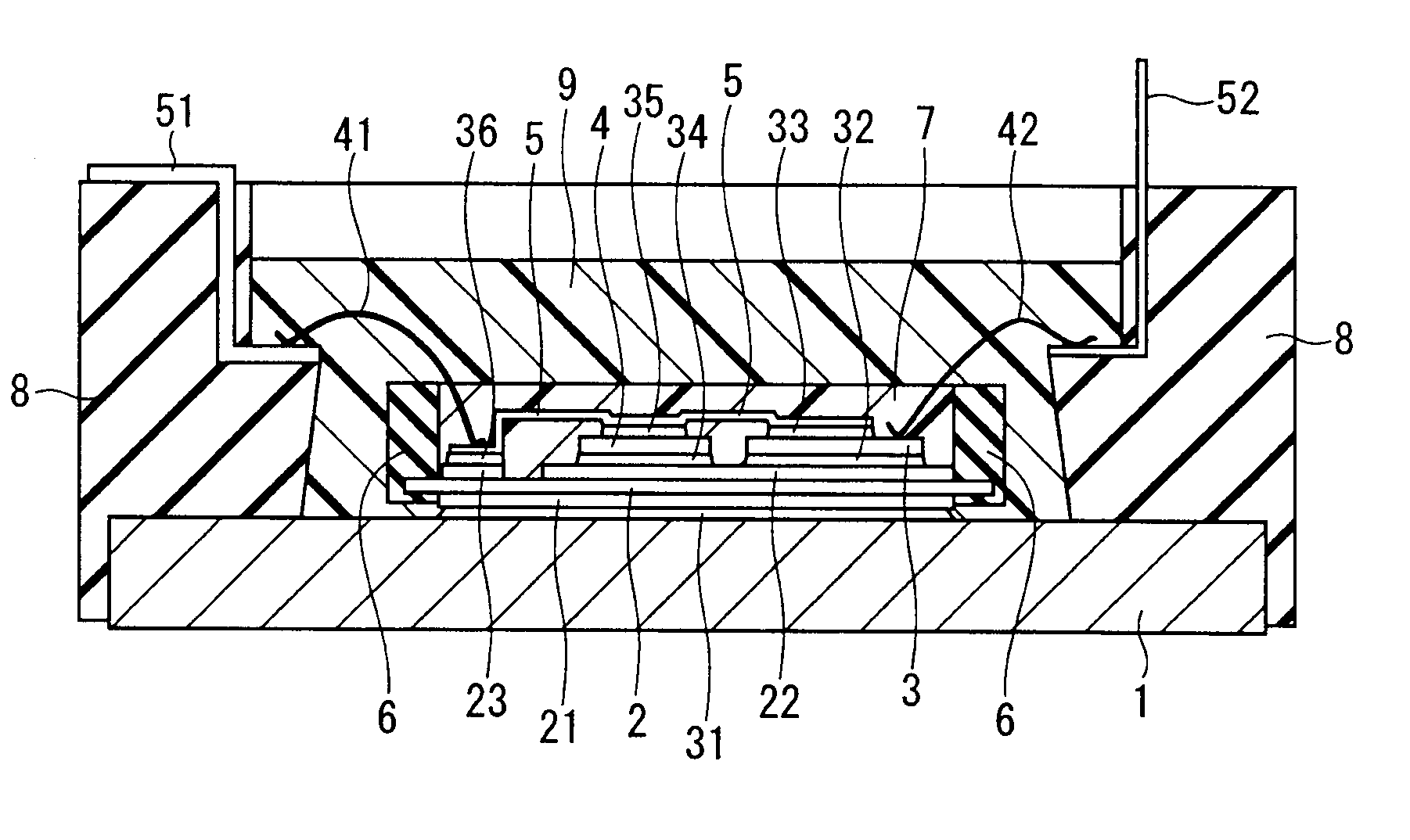
[0021]FIG. 1 is a sectional view showing the structure of a semiconductor module of a first preferred embodiment. The semiconductor module includes a base plate 1 made of metal such as copper, aluminum and AlSiC, and an insulating substrate joined onto the base plate 1 through solder 31. The structure of the insulating substrate is such that patterns of metal such as copper or aluminum are formed on opposite sides of a ceramic insulating plate 2 by etching technique. A metal pattern 21 is formed on the rear surface of the insulating plate 2, and the metal pattern 21 is joined through solder 31 to the base plate 1. Metal patterns 22 and 23 are formed on the front surface of the insulating plate 2. A power device chip 3 that may be an IGBT or an MOSFET, and a free-wheeling diode chip 4 are joined on the metal pattern 22 through solder 32 and solder 34 respectively.

[0022]A lead frame 5 is joined on the power device chip 3 and the free-wheeling diode chip 4 through solder 33 and solder ...

second preferred embodiment

Structure

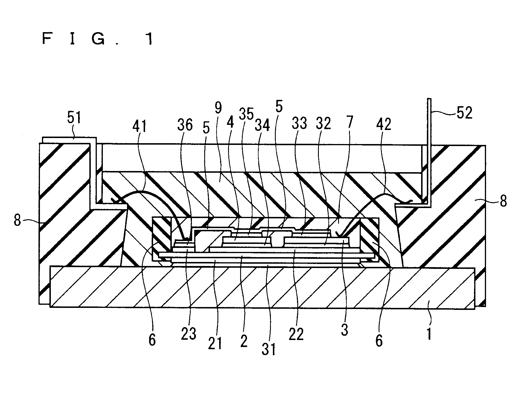
[0029]It been confirmed by experiment that insulation degradation is generated with high probability between different electrodes. So, in a second preferred embodiment, only a single metal pattern is formed on the insulating plate 2 to maintain a single potential to enhance insulation properties.

[0030]FIG. 2 is a sectional view showing the structure of a semiconductor module of the second preferred embodiment. In this semiconductor module, only the metal pattern 22 is formed on the insulating plate 2, and the power device chip 3 and the free-wheeling diode chip 4 are joined on the metal pattern 22 through the solder 32 and the solder 34 respectively. Further, an insulating spacer 10 is joined through solder 37 to an end portion of the metal pattern 22 away from the power device chip 3. The lead frame 5 is joined through the solder 36 on the insulating spacer 10. The insulating spacer 10 is provided to insulate the lead frame 5 from the metal pattern 22. The insulating space...

third preferred embodiment

Structure

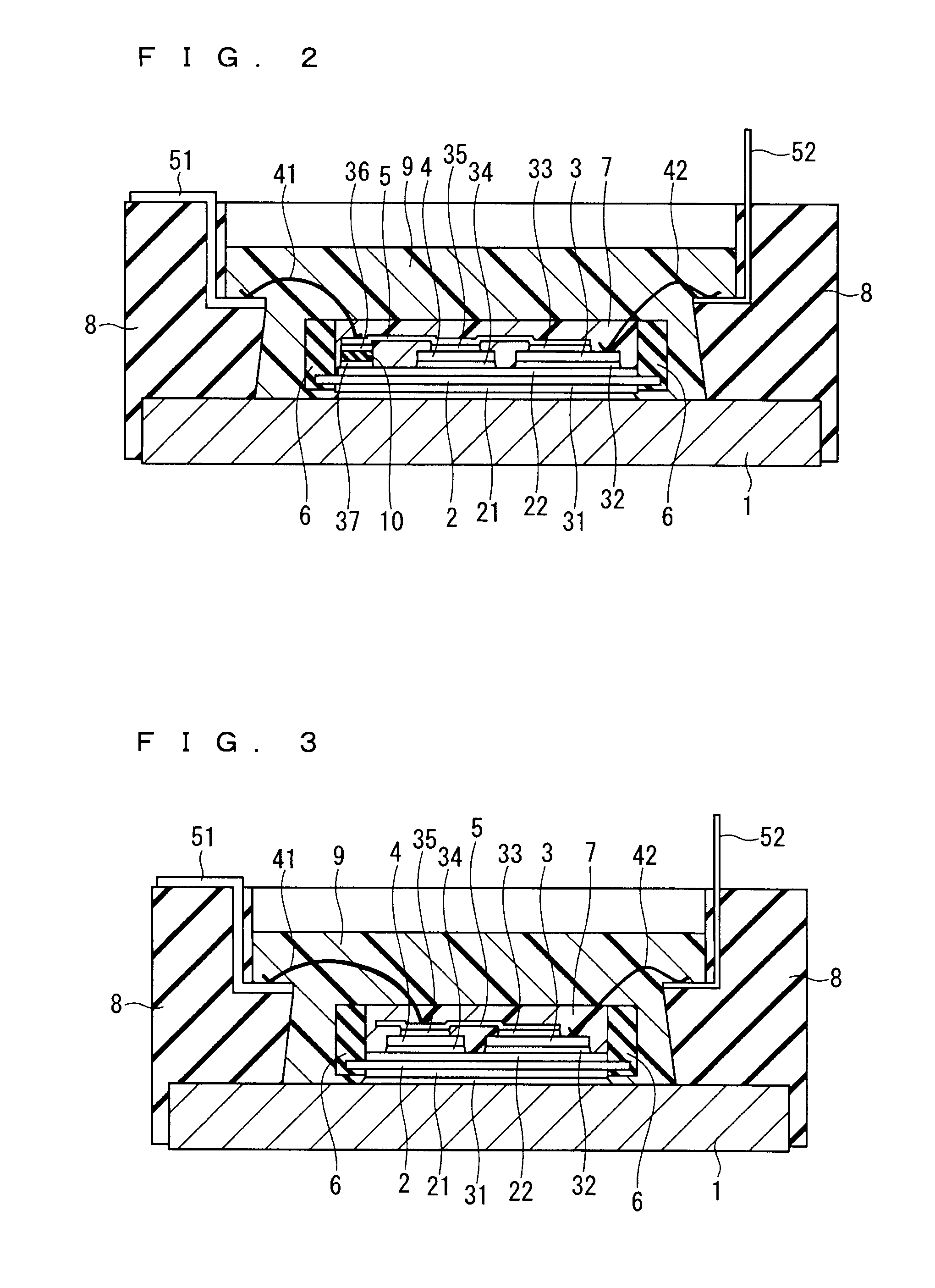
[0034]FIG. 3 is a sectional view showing the structure of a semiconductor module of a third preferred embodiment. The third preferred embodiment is intended to reduce the size of the semiconductor module by making the size of the lead frame 5 smaller than those in the first and second preferred embodiments.

[0035]The metal pattern 22 is formed on a surface of the insulating plate 2. The power device chip 3 and the free-wheeling diode chip 4 are joined on the metal pattern 22 through the solder 32 and the solder 34 respectively.

[0036]The lead frame 5 is joined on the power device chip 3 that may be an IGBT or an MOSFET and the free-wheeling diode chip 4 through the solder 33 and the solder 35 respectively to connect the power device chip 3 and the free-wheeling diode chip 4 in parallel. The lead frame 5 is connected through the aluminum wire 41 to the external main electrode 51 above the free-wheeling diode chip 4. The free-wheeling diode chip 4 increases in temperature at a ...


PUM


Abstract

A semiconductor module includes: an insulating plate; a plurality of metal patterns formed on the insulating plate and spaced apart from each other; a power device chip solder-joined on one the metal pattern; a lead frame solder-joined on the metal pattern to which the power device chip is not solder-joined, and on the power device chip; an external main electrode provided to an outer casing, and joined by wire bonding to the lead frame above the metal pattern to which the power device chip is not joined; and a sealing resin formed by potting to seal the power device chip, the lead frame, and the metal patterns.

Description

BACKGROUND OF THE INVENTION[0001]1. Field of the Invention[0002]The present invention relates to a semiconductor module, and more specifically, relates to a structure for connecting a power device chip and an external electrode.[0003]2. Description of the Background Art[0004]A technique called wire bonding has been employed since 1980s as means of taking current out of a power device (see Japanese Patent Application Laid-Open No. 2010-238892). In the wire bonding technique, an electrode part of the power device and an external electrode are connected by using a thin aluminum or gold wire. However, this technique shortens the life span of a joint part formed by wire bonding due to heat stress generated by turning the power device on and off repeatedly. So, the maximum junction temperature should be set low if increase of a life span is given higher priority, resulting in the size increase or cost increase of a power module.[0005]In response, direct lead bonding (DLB) technique has be...

Claims


Application Information

Patent Timeline
Patent Type & Authority Applications(United States)
IPC IPC(8): H01L23/495B82Y99/00
CPCH01L23/24H01L2224/40137H01L23/3735H01L23/4334H01L24/48H01L2224/32225H01L2224/48472H01L2224/73265H01L2924/13091H01L2224/45144H01L23/3135H01L23/4952H01L2224/8384H01L2224/48091H01L2224/29339H01L2924/01029H01L2224/40227H01L2224/40139H01L2924/13055H01L2224/73221H01L2224/73215H01L2224/48227H01L2224/45124H01L2224/33181H01L2224/32245H01L2224/291H01L25/072H01L24/73H01L24/45H01L24/40H01L2924/19107H01L24/29H01L24/32H01L24/33H01L2924/00012H01L2924/014H01L2924/00H01L2924/00014H01L2224/45015H01L2924/351H01L2224/40095H01L2924/181H01L2224/40225H01L2224/84801H01L24/37H01L2224/37147H01L2224/83801H01L24/84
Inventor OTA, TATSUOSHINOHARA, TOSHIAKI
Owner MITSUBISHI ELECTRIC CORP
Why Eureka
Try Eureka