Method for fabricating silicon nanowire arrays

a silicon nanowire array and silicon nanowire technology, applied in nanotechnology, material nanotechnology, semiconductor devices, etc., can solve the problems of high manufacturing cost, difficult to fabricate silicon nanowire arrays with a large area such as solar panels, and poor uniformity of formed silicon nanowire arrays, so as to reduce the etching rate of forming silicon nanowires

Inactive Publication Date: 2013-01-10
NAT TAIWAN UNIV OF SCI & TECH
View PDF2 Cites 20 Cited by
  • Summary
  • Abstract
  • Description
  • Claims
  • Application Information

AI Technical Summary

Benefits of technology

[0010]It is worth mentioning that the length of the formed silicon nanowires is smaller than or equal to an etching depth of the silicon material. The smaller an area of the metal layer on

Problems solved by technology

However, the manufacturing cost thereof is higher, and it is difficult to fabricate the silicon nanowire array with a large area such solar panels.
However, in fabricating the silicon nanowire arrays by the conventional metal-induced silicon etching, sizes and locations of deposited metal particles are random,

Method used


Image

  • Method for fabricating silicon nanowire arrays
  • Method for fabricating silicon nanowire arrays
  • Method for fabricating silicon nanowire arrays

Examples


Embodiment Construction

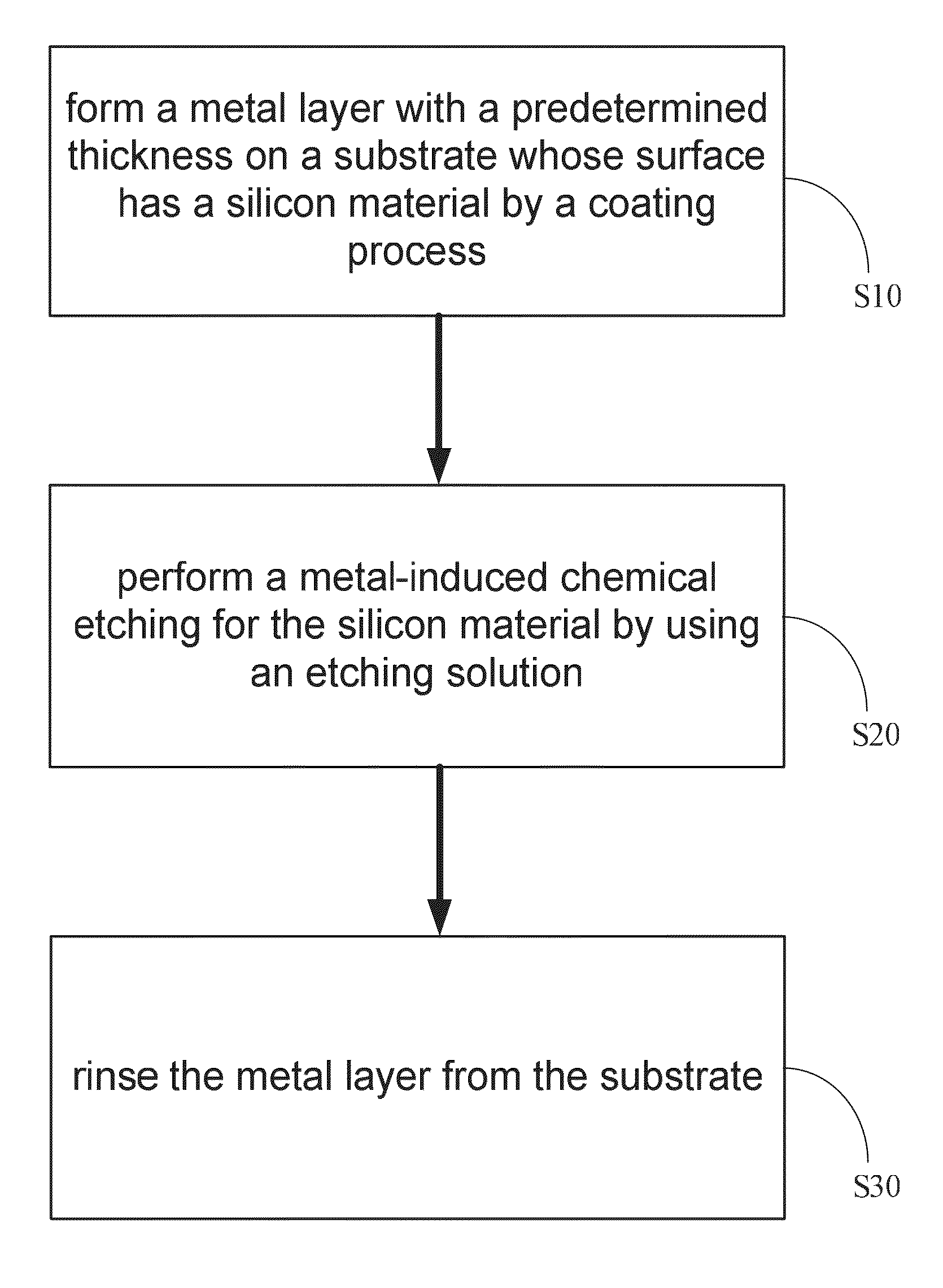
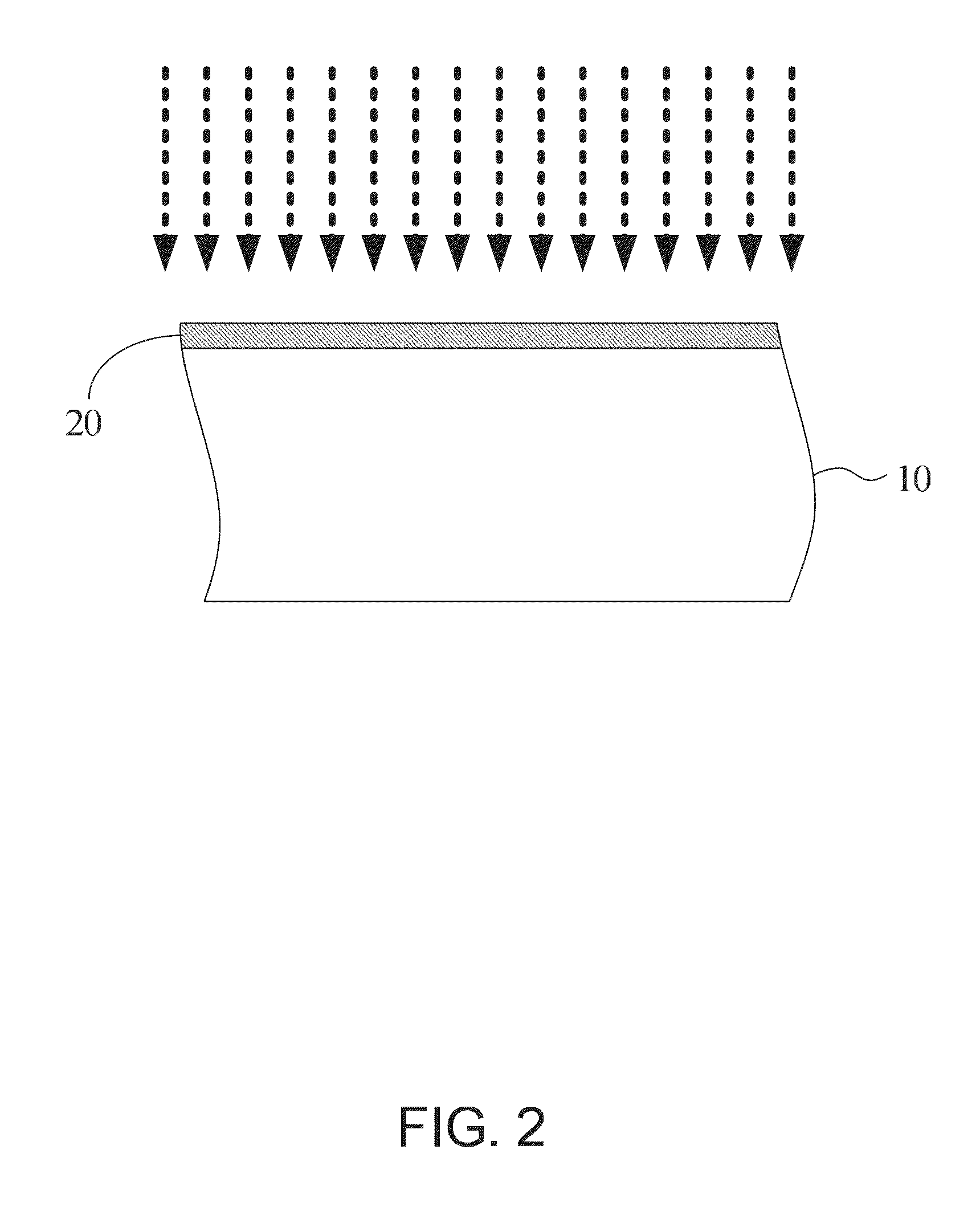
[0022]The following will explain a method for fabricating silicon nanowire arrays according to a preferred embodiment of the present invention in detail with drawings. Referring to FIG. 1 and FIG. 2, FIG. 1 depicts a flow chart illustrating a method for fabricating silicon nanowire arrays according to the preferred embodiment of the present invention, and FIG. 2 depicts a schematic cross-sectional diagram illustrating a substrate whose surface has a silicon material in performing step S10. The fabricating method is utilized to fabricate a silicon nanowire array with a high uniformity on a substrate whose surface has a silicon material, or substrate 10 for short. The silicon material herein can be a monocrystalline silicon, which has a lattice plane of (100), (110), or (111). The silicon material also can be a polycrystalline silicon or amorphous silicon (a-Si); moreover, the silicon material is intrinsic silicon or doped silicon.

[0023]At step S10, a metal layer 20 with a predetermin...


PUM


Abstract

A method for larger-area fabrication of uniform silicon nanowire arrays is disclosed. The method includes forming a metal layer with a predetermined thickness on a substrate whose surface has a silicon material by a coating process, the metal layer selected from the group consisting of Ag, Au and Pt; and performing a metal-induced chemical etching for the silicon material by using an etching solution. Accordingly, a drawback that Ag nanoparticles are utilized to perform the metal-induced chemical etching in prior art is solved.

Description

CROSS-REFERENCE[0001]This application claims the priority of Taiwan Patent Application No. 100123562, filed on Jul. 4, 2011. This invention is partly disclosed in a conference “WTM 2011 IEEE Photonics Society Winter Topical Meeting on Low Dimensional Nanostructures and Sub-Wavelength Photonics, 10 Jan. 2011”, entitled “Aligned Silicon Nanowire Arrays for Achieving Black Nonreflecting Silicon Surface” completed by Yung-jr Hung, Kai-chung Wu, San-hang Lee.TECHNICAL FIELD OF THE INVENTION[0002]The present invention relates to a method for fabricating silicon nanowires, especially to a method for larger-area fabrication of uniform silicon nanowire arrays.BACKGROUD OF THE INVENTION[0003]Silicon nanowire (SiNW) arrays have an antireflective surface, and it can be applied to surfaces of solar cells for effectively enhancing the absorption of sunlight. Conventionally, the silicon nanowire (SiNW) arrays are fabricated by photolithigraphy processes. However, the manufacturing cost thereof is ...

Claims


Application Information

Patent Timeline
IPC IPC(8): H01L21/28B82Y40/00
CPCH01L29/0669B82Y40/00B82Y30/00Y02E10/50H01L31/035227B82Y20/00H01L31/02363
Inventor HUNG, YUNG-JRLEE, SAN-LIANGWU, KAI-CHUNG
Owner NAT TAIWAN UNIV OF SCI & TECH
Why Eureka
Try Eureka