Metal oxide semiconductor transistor and method of manufacturing the same

Active Publication Date: 2013-01-24
UNITED MICROELECTRONICS CORP
View PDF0 Cites 22 Cited by
  • Summary
  • Abstract
  • Description
  • Claims
  • Application Information

AI Technical Summary

Benefits of technology

[0031]In the method for manufacturing the MOS transistor of the present invention, the dielectric barrier layer is formed on the barrier layer on the high-k dielectric layer. When the first work function metal layer in the second MOS region is removed by using a wet etching process, the dielectric barrier layer such as the silicon nitride layer can not be etched by an etchant of the wet etching process. Thus, the dielectric barrier layer is an effective etch stop layer during removing the first work function metal layer in the second MOS region. Meanwhile, a suitable process, for example, a dry etching process can etch the dielectric barrier layer such as the silicon nitride layer, but can barely etch the barrier layer such as the titanium nitride layer. Therefo

Problems solved by technology

However, in the typical method for manufacturing the metal gate, the high-k dielectric layer is prone to be etched by the etchants used during forming the metal gate so as to

Method used


Image

  • Metal oxide semiconductor transistor and method of manufacturing the same
  • Metal oxide semiconductor transistor and method of manufacturing the same
  • Metal oxide semiconductor transistor and method of manufacturing the same

Examples


Embodiment Construction

[0036]The present invention will now be described more specifically with reference to the following embodiments. It is to be noted that the following descriptions of preferred embodiments of this invention are presented herein for purpose of illustration and description only. It is not intended to be exhaustive or to be limited to the precise form disclosed.

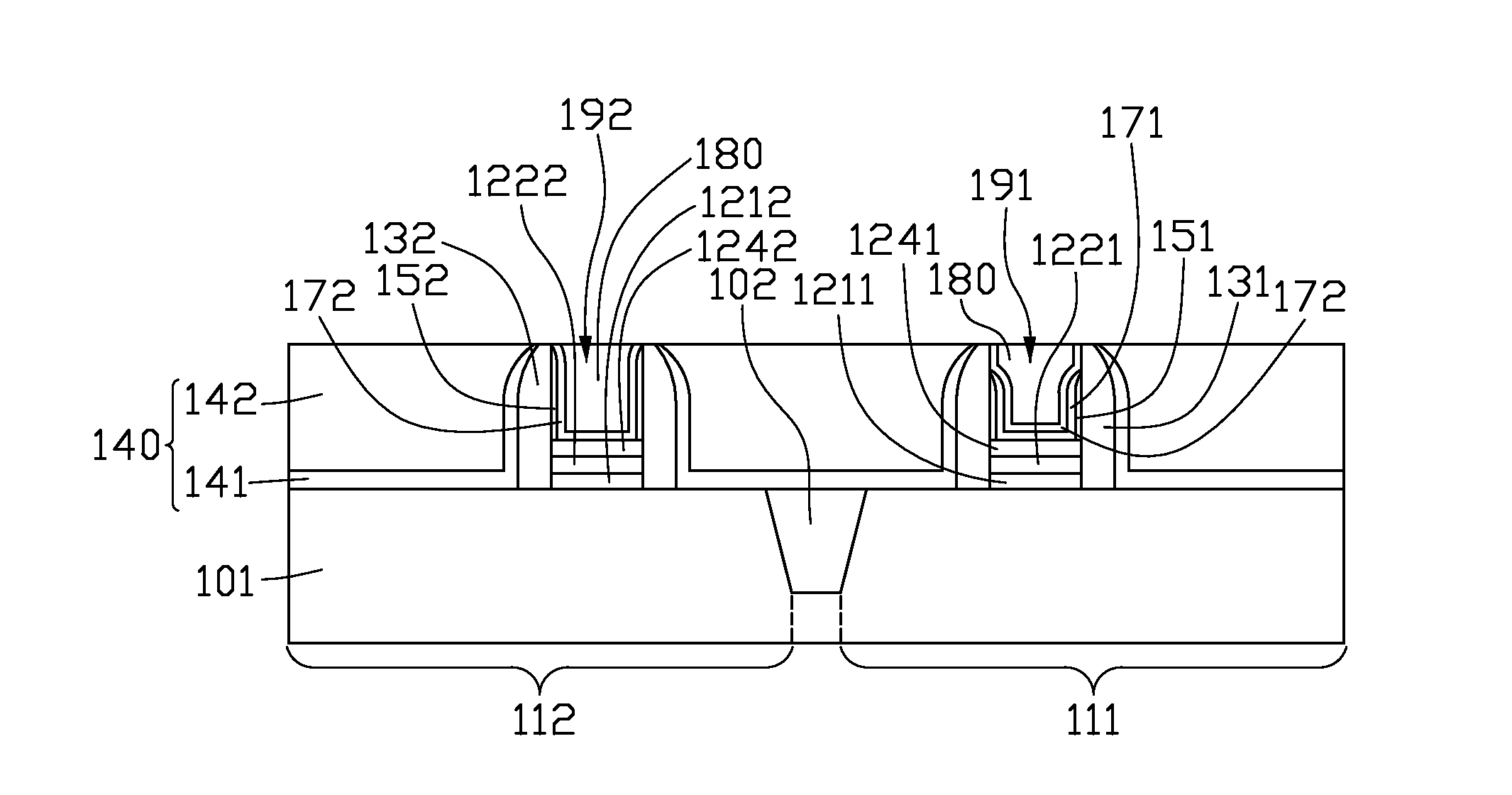
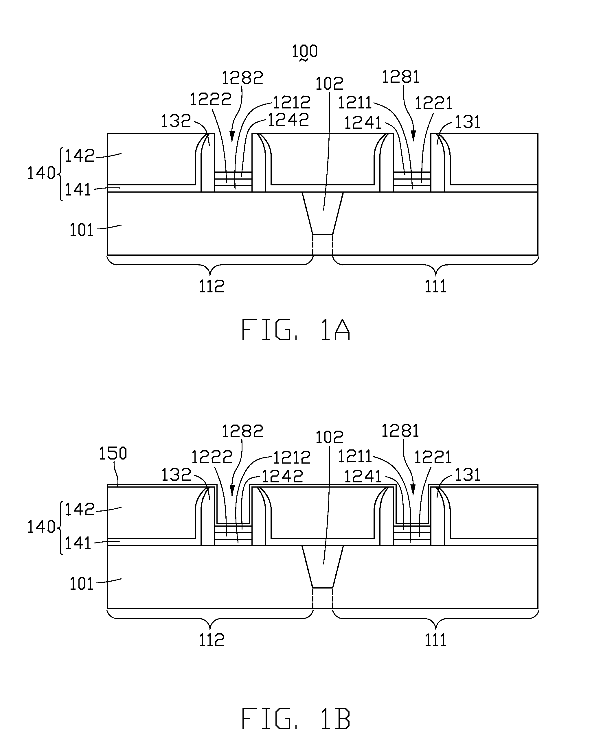
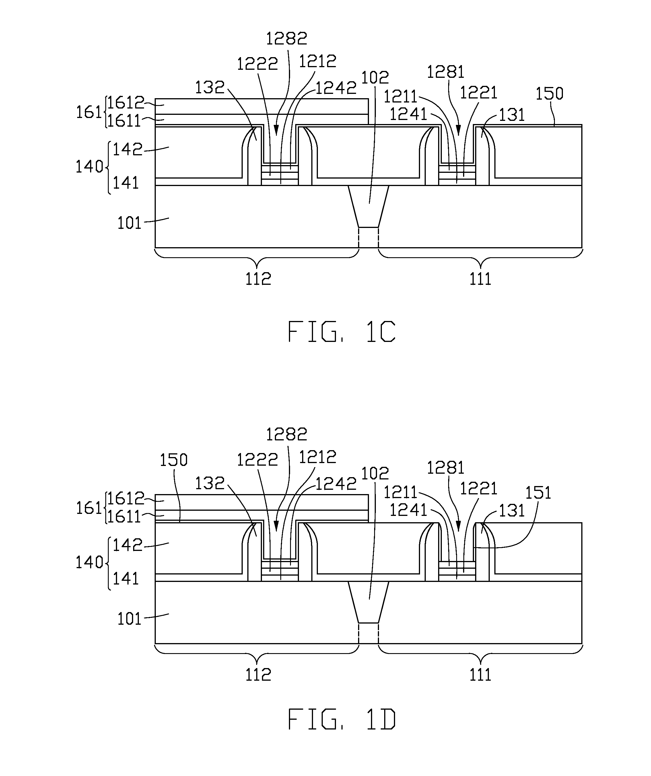
[0037]FIGS. 1A-1N illustrate a partial process flow of a method for manufacturing a MOS transistor in accordance with first embodiment of the present invention. In the present embodiment, a high-k first process (i.e., a high-k dielectric layer is firstly formed before removing a poly-silicon dummy gate) is, but not limited to, used as an example to describe the method for manufacturing a MOS transistor. In other words, a MOS transistor includes any gate structure having the high-k dielectric layer can utilize the method for manufacturing a MOS transistor.

[0038]Referring to FIG. 1A, a substrate 100 is formed by the following steps...


PUM


Abstract

A method for manufacturing a MOS transistor is provided. A substrate has a high-k dielectric layer and a barrier in each of a first opening and a second opening formed by removing a dummy gate and located in a first transistor region and a second transistor region. A dielectric barrier layer is formed on the substrate and filled into the first opening and the second opening to cover the barrier layers. A portion of the dielectric barrier in the first transistor region is removed. A first work function metal layer is formed. The first work function metal layer and a portion of the dielectric barrier layer in the second transistor region are removed. A second work function metal layer is formed. The method can avoid a loss of the high-k dielectric layer to maintain the reliability of a gate structure, thereby improving the performance of the MOS transistor.

Description

FIELD OF THE INVENTION[0001]The present invention relates to a metal oxide semiconductor (MOS) transistor, and particularly to a MOS transistor including a gate structure with a high-k dielectric layer and a method for manufacturing the same.BACKGROUND OF THE INVENTION[0002]In a fabrication of an integrated circuit, for example, a MOS transistor, a gate structure including a high-k dielectric layer and a metal gate (hereafter called HK / MG for short) has been widely used so as to improve the performance of the integrated circuit.[0003]Generally, in the technology for manufacturing the HK / MG, after a poly-silicon dummy gate is removed, the metal gate of the HK / MG is formed. The high-k dielectric layer can be formed before removing the poly-silicon dummy gate (High-K first) or after removing the poly-silicon dummy gate (High-K last). However, in the typical method for manufacturing the metal gate, the high-k dielectric layer is prone to be etched by the etchants used during forming the...

Claims


Application Information

Patent Timeline
IPC IPC(8): H01L29/78H01L21/76H01L21/28
CPCH01L21/823842H01L21/823864H01L21/28088H01L29/4966H01L29/78H01L29/66545H01L29/66553H01L29/6659H01L29/7833H01L29/513
Inventor LU, TSUO-WENLEE, TZUNG-YINGCHEN, JEI-MINGHSU, CHUN-WEILIN, YU-MINCHANG, CHIA-LUNGCHIEN, CHIN-CHENGCHAN, SHU-YEN
Owner UNITED MICROELECTRONICS CORP
Why Eureka
Try Eureka