Boron-Containing Buffer Layer for Growing Gallium Nitride on Silicon

a gallium nitride and buffer layer technology, applied in the direction of basic electric elements, electrical apparatus, semiconductor devices, etc., can solve the problems of reducing gan is not well suited for epitaxial growth directly on a silicon substrate, and the boron-containing buffer layer is a costly manufacturing step, so as to reduce the size of the wurtzite-type crystal latti

Inactive Publication Date: 2013-01-31
KK TOSHIBA
View PDF1 Cites 50 Cited by
  • Summary
  • Abstract
  • Description
  • Claims
  • Application Information

AI Technical Summary

Benefits of technology

[0015]A device used in manufacturing LEDs includes a silicon substrate, a wurtzite-type crystal lattice including aluminum and nitrogen atoms, and a means for reducing the size of the wurtzite-type crystal lattice. The substrate of silicon has an Si(111) surface. A silicon crystal lattice is present across the Si(111) surface with cell units of a first length. The wurtzite-type crystal lattice has a C-plane that is parallel to the Si(111) surface, and cell units in the C-plane having a second length. The means is incorporated into the wurtzite-type crystal lattice and decreases the second length of the cell units of the wurtzite-type crystal lattice such that three times the second length equals twice the first length.

Problems solved by technology

Current attempts to grow high quality epitaxial layers of GaN on silicon substrates, however, have not been entirely successful.
Because of the great difference between the lattice constants and thermal expansion coefficients of GaN and silicon, GaN is not well suited for epitaxial growth directly on a silicon substrate.
Growing the buffer layers is a costly manufacturing step not only because of the materials used in the buffer layers but also because of the additional time required to grow the buffer layers.
Moreover, the quality of the epitaxial GaN layers that can be grown over existing buffer layers has been poor.
Current methods of forming buffer layers of AlN and AlGaN have resulted in epitaxial growth of GaN layers that contain structural defects such as discontinuities, dislocations and faults.
These defects degrade the morphology and optical properties of the GaN layers, rendering the GaN layers unsuitable for use in high quality LEDs.

Method used


Image

  • Boron-Containing Buffer Layer for Growing Gallium Nitride on Silicon
  • Boron-Containing Buffer Layer for Growing Gallium Nitride on Silicon
  • Boron-Containing Buffer Layer for Growing Gallium Nitride on Silicon

Examples


first embodiment

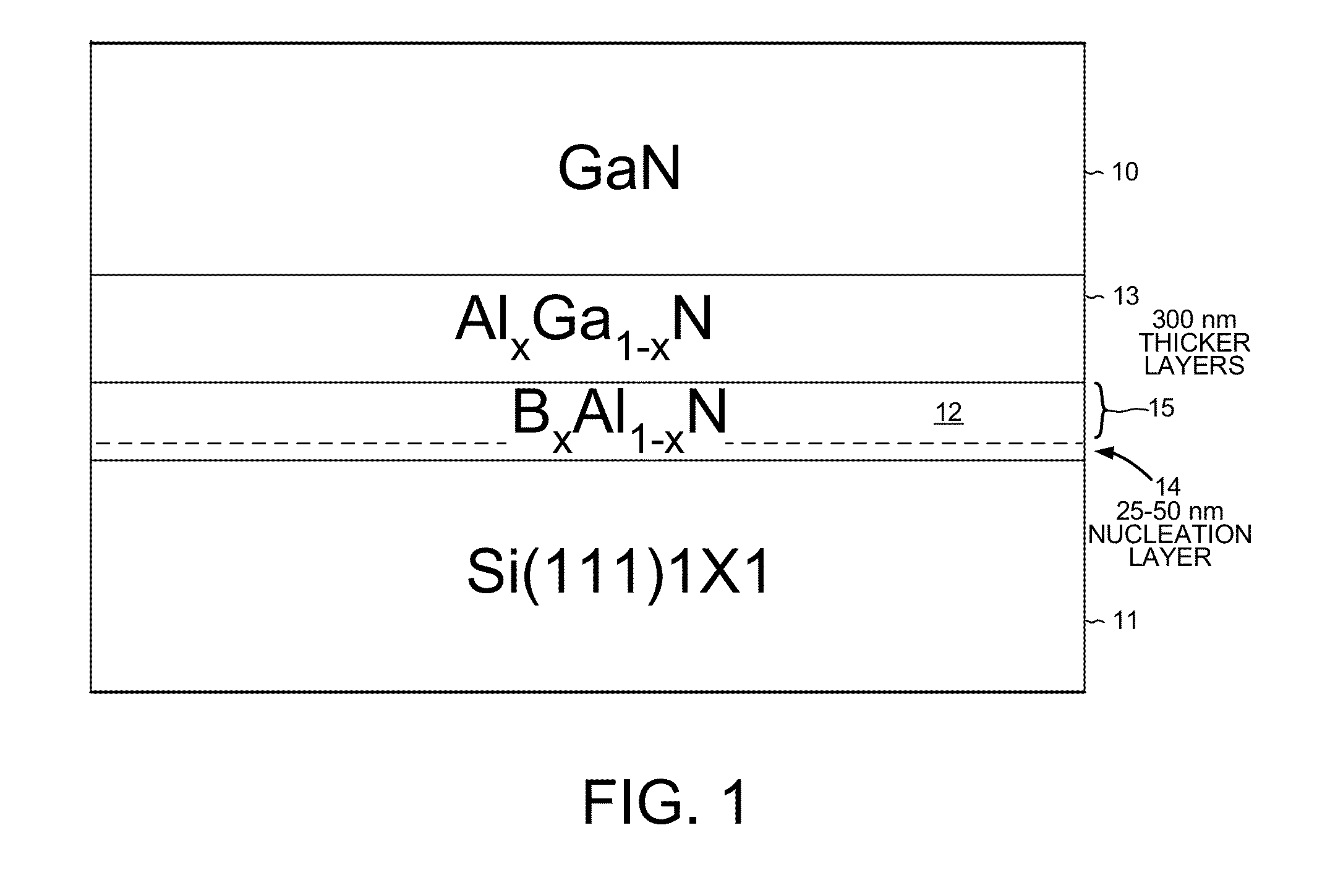
[0034]FIG. 1 is a schematic diagram showing the growth of a single crystal GaN layer 10 on buffer layers over a silicon substrate 11 in the present invention. A buffer layer of boron-aluminum nitride (BxAl1-xN) 12 is first grown on the silicon substrate 11. Then higher buffer layers of aluminum gallium nitride (AlxGa1-xN) 13 are grown over the boron-aluminum nitride layer 12. Finally, the GaN layer 10 is grown over the top layer of aluminum gallium nitride 13. In some embodiments, the GaN layer includes several sublayers. The buffer layer of boron-aluminum nitride 12 is made up of a lower initial nucleation layer 14 and thicker upper layers 15.

[0035]There are several reasons for first growing buffer layers on a silicon substrate before the gallium nitride (GaN) layer 10 is grown. First, meltback etching of the silicon substrate 11 by gallium occurs if the gallium is allowed to react directly with the silicon substrate. The reaction between gallium and silicon results in poor crystal...

second embodiment

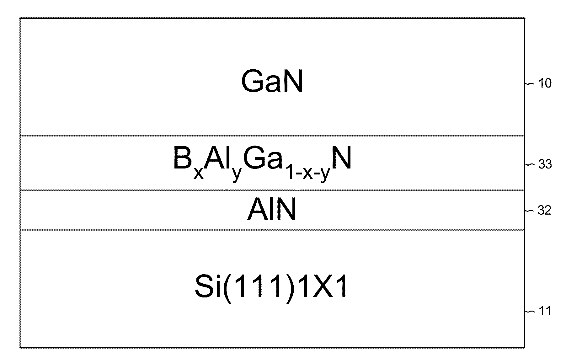
[0073]FIG. 14 is a schematic diagram showing the growth of single crystal GaN layer 10 on buffer layers over a silicon substrate 11 in the present invention. A buffer layer of aluminum nitride (AlN) 32 is first grown on the silicon substrate 11. Then higher buffer layers of boron aluminum gallium nitride (BxAlyGa1-x-yN) 33 are grown over the aluminum nitride layer 32. Finally, the GaN layer 10 is grown over the top layer of boron aluminum gallium nitride 33.

[0074]By adding boron to reduce the lattice size of AlGaN, more compressive stress can be built up in thinner BAlGaN layers between the AlN and the GaN. The smaller lattice size of the BAlGaN crystal is used to build up compressive stress by growing successive buffer layers of boron aluminum gallium nitride (BxAlyGa1-x-yN) 33 with increasingly larger lattice sizes. The lowest BAlGaN buffer layer has the most amount of boron and least amount of gallium, which produces the shortest cell unit length. The composition of each higher b...

third embodiment

[0075]In a third embodiment, boron gallium nitride (BxGa1-xN) is used instead of boron aluminum gallium nitride (BxAlyGa1-x-yN) as a buffer between the AlN layer and the GaN layer. The lowest BGaN buffer layer has the most amount of boron and the least amount of gallium. The composition of each higher buffer layer of BGaN contains more gallium and less boron in order to generate ever larger lattice sizes.


PUM

PropertyMeasurementUnit
thickaaaaaaaaaa
diameteraaaaaaaaaa
diameteraaaaaaaaaa

Abstract

A silicon wafer used in manufacturing GaN for LEDs includes a silicon substrate, a buffer layer of boron aluminum nitride (BxAl1-xN) and an upper layer of GaN, for which 0.35≦x≦0.45. The BAlN forms a wurtzite-type crystal with a cell unit length about two-thirds of a silicon cell unit length on a Si(111) surface. The C-plane of the BAlN crystal has approximately one atom of boron for each two atoms of aluminum. Across the entire wafer substantially only nitrogen atoms of BAlN form bonds to the Si(111) surface, and substantially no aluminum or boron atoms of the BAlN are present in a bottom-most plane of atoms of the BAlN. A method of making the BAlN buffer layer includes preflowing a first amount of ammonia equaling less than 0.01% by volume of hydrogen flowing through a chamber before flowing trimethylaluminum and triethylboron and then a subsequent amount of ammonia through the chamber.

Description

TECHNICAL FIELD[0001]The present invention relates generally to methods of growing gallium nitride on silicon.BACKGROUND INFORMATION[0002]Thin films of Group III nitride, such as gallium nitride (GaN), are used in the production of efficient optoelectronic light emitters. Conventionally, GaN has been grown directly on sapphire substrates (Al2O3). The GaN is grown in thin layers as opposed to in a single three-dimensional growth mode in order to achieve a high quality crystalline structure of the epitaxial growth. Growing the epitaxial layers of GaN on silicon as opposed to on sapphire offers considerable cost savings because of the economies of scale from the large production of silicon for the semiconductor industry. A large amount of equipment for the production of crystalline silicon has already been depreciated. That equipment can now be used in the production of light emitting diodes (LEDs).[0003]Current attempts to grow high quality epitaxial layers of GaN on silicon substrate...

Claims


Application Information

Patent Timeline
Patent Type & Authority Applications(United States)
IPC IPC(8): H01L29/205H01L29/04H01L21/20
CPCH01L21/02381H01L21/02458H01L21/02502H01L33/007H01L21/0262H01L29/267H01L21/0254
Inventor FENWICK, WILLIAM E.
Owner KK TOSHIBA
Why Eureka
Try Eureka