Display element, display device, and projection display device

a display element and display device technology, applied in the field of display elements, can solve the problems of improper directivity of light emitted, difficulty in narrowing the emission angle of light emitted from the display element to less than 15°, etc., and achieve the effect of high directivity and high luminan

Active Publication Date: 2013-01-31
NEC CORP
View PDF10 Cites 7 Cited by
  • Summary
  • Abstract
  • Description
  • Claims
  • Application Information

AI Technical Summary

Benefits of technology

[0017]According to the present invention, since both luminance and directivity of light that is emit

Problems solved by technology

However, it is difficult to narrow the emission angle of light emitted from the display element to less than ±15°.
In other

Method used


Image

  • Display element, display device, and projection display device
  • Display element, display device, and projection display device
  • Display element, display device, and projection display device

Examples


first embodiment

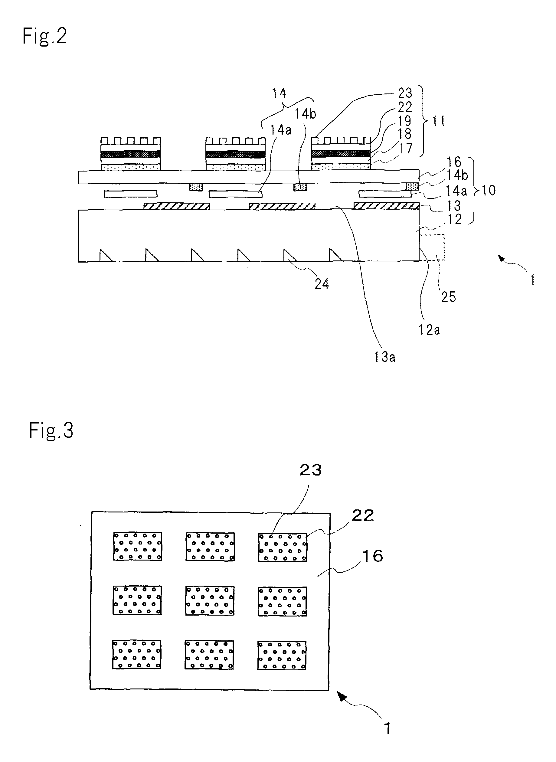
[0045]FIG. 2 is a sectional view schematically showing a display element according to a first embodiment of the present invention. Since the individual layers of the display element are very thin and their thickness largely differs, it is difficult to illustrate the individual layers in exact scale. Thus, the drawings do not illustrate the individual layers in exact scale, but schematically illustrate them.

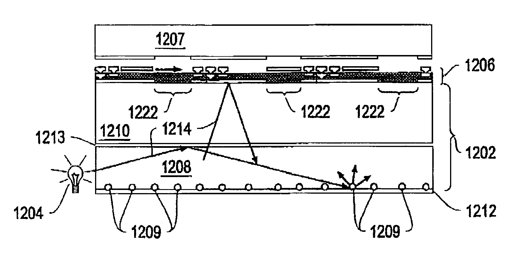
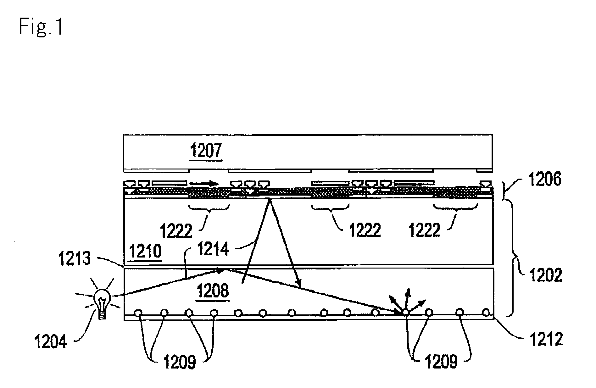
[0046]As shown in FIG. 2, display element 1 according to this embodiment has light valve section 10 including a plurality of shutter mechanisms 14 as a plurality of optical shutter means that switch between a transmitting state and a shading state of light emitted from light emitting element 25 and substrate 16 through which light that exits shutter mechanisms 14 is transmitted. In addition, display element 1 has a plurality of plasmon coupling sections 11 that cause plasmon coupling to occur with light that exits light valve section 10.

[0047]Light valve section 10 has light condu...

second embodiment

[0088]FIG. 7 is a sectional view schematically showing a display element according to a second embodiment of the present invention. The display element according to the second embodiment is different from display element 1 according to the first embodiment in the structure of plasmon coupling sections. In display element 1 according to the foregoing first embodiment, light excited in plasmon excitation layer 19 exits wave number vector conversion layer 23. The display element according to the second embodiment is different from that according to the first embodiment in that surface plasmons that occur in the plasmon excitation layer exit the wave number vector conversion layer as light. The effective dielectric constant of the incident side portion of the plasmon excitation layer is set to be higher than the effective dielectric constant of the exit side portion of the plasmon excitation layer.

[0089]As shown in FIG. 7, plasmon coupling sections 21 of display element 2 according to t...

third embodiment

[0098]FIG. 8 is a sectional view schematically showing a display element according to a third embodiment of the present invention. The display element according to the third embodiment is different from display element 1 according to the first embodiment as regards the structure of plasmon coupling sections.

[0099]As shown in FIG. 8, plasmon coupling sections 31 of display element 3 according to the third embodiment have a stacked structure in which base layer 28, carrier generation layer 37, and plasmon excitation layer 39 are successively stacked on substrate 16 of light valve section 10. Plasmon excitation layer 39 according to the third embodiment has periodic structure 39a that has the functions of the foregoing wave number vector conversion layers 23 and 33. Periodic structure 39a has a one-dimensional or two-dimensional grating structure (uneven structure). Likewise, base layer 28 and carrier generation layer 37 have a periodic structure in the shape of periodic structure 39a ...


PUM


Abstract

The present invention includes light valve section (10) having a plurality of shutter mechanisms (14) that switch between a transmitting state and a shading state of light emitted from light emitting element (25); and substrate (16) through which light that exits plurality of shutter mechanisms (14) is transmitted. The display element also has plasmon coupling section (11) that causes plasmon coupling to occur with light that exits the light valve section (10). Plasmon coupling section (11) includes carrier generation layer (17) that generates carriers with incident light that exits light valve section (10), plasmon excitation layer (19) that has a higher plasma frequency than the frequency of light that is generated in carrier generation layer (17) excited with the light emitted from light emitting element (25), and wave number vector conversion layer (22) that converts the light or surface plasmons generated in plasmon excitation layer (19) into light having a predetermined exit angle. Plasmon excitation layer (19) is sandwiched between first dielectric constant layer (18) and second dielectric constant layer (22).

Description

TECHNICAL FIELD[0001]The present invention relates to a display element, a display device, and a projection display device that use surface plasmons to emit light.BACKGROUND ART[0002]A projector having solid state light source that uses a light emitting element such as a light emitting diode (LED) or a semiconductor laser (LD) as a light source has been proposed. A projector having solid state light source of this type has an illumination optical system into which light emitted from the light emitting element enters; a light valve having a display element such as a liquid crystal display panel that light that exits the illumination optical system enters or a DMD (Digital Micromirror Device); and a projection optical system that projects light that exits the light valve to a projection plane.[0003]A requirement for the projector, having solid state light source, is that there be a minimum of optical loss in the optical path from the light emitting element to the light valve so as to ...

Claims


Application Information

Patent Timeline
IPC IPC(8): H05B33/22H05B33/14G02F1/13357G03B21/14
CPCG02B5/008G02F2203/10G02B6/005G02B6/0075G02B26/02G03B21/00G03B21/14G03B21/20G03B21/28H04N9/3152G03B21/204G03B21/2066G02F2/02G02F2202/32G02B6/0038G03B21/005
Inventor NATSUMEDA, MASANAOIMAI, MASAOSAITOH, GOROHTOMINAGA, SHIN
Owner NEC CORP
Why Eureka
Try Eureka