

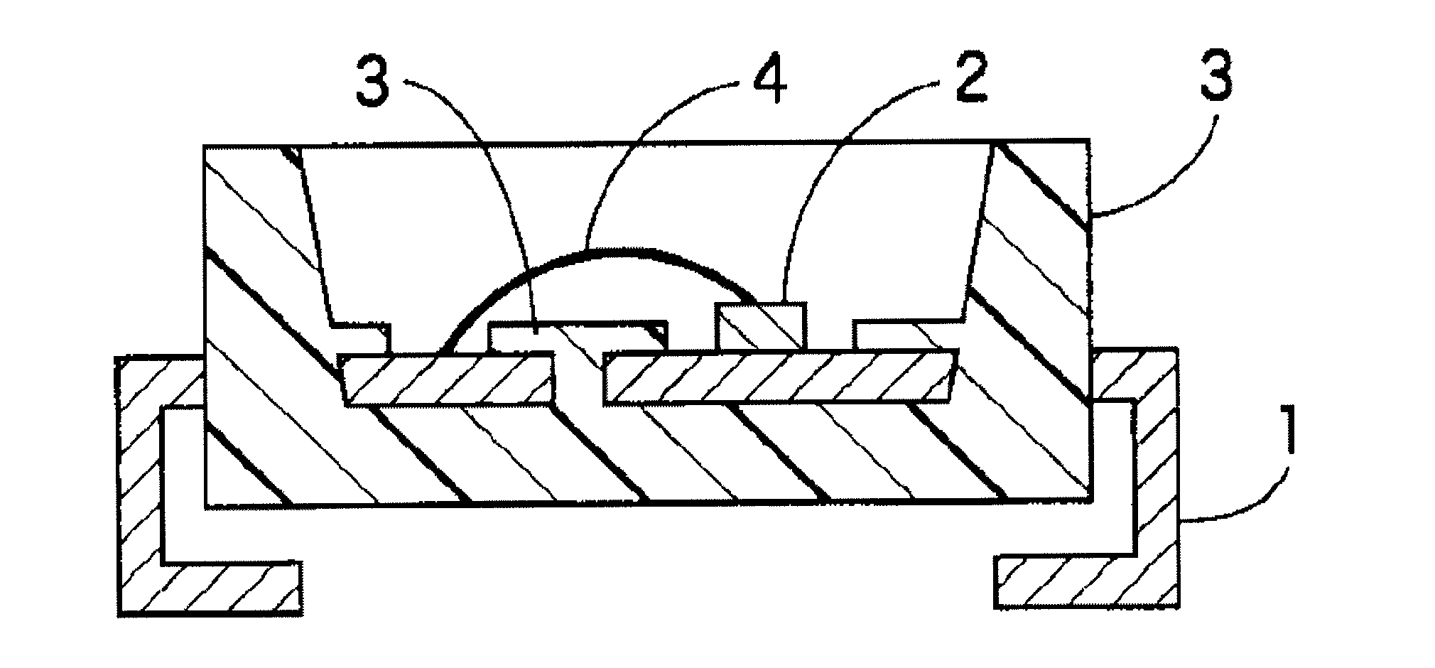
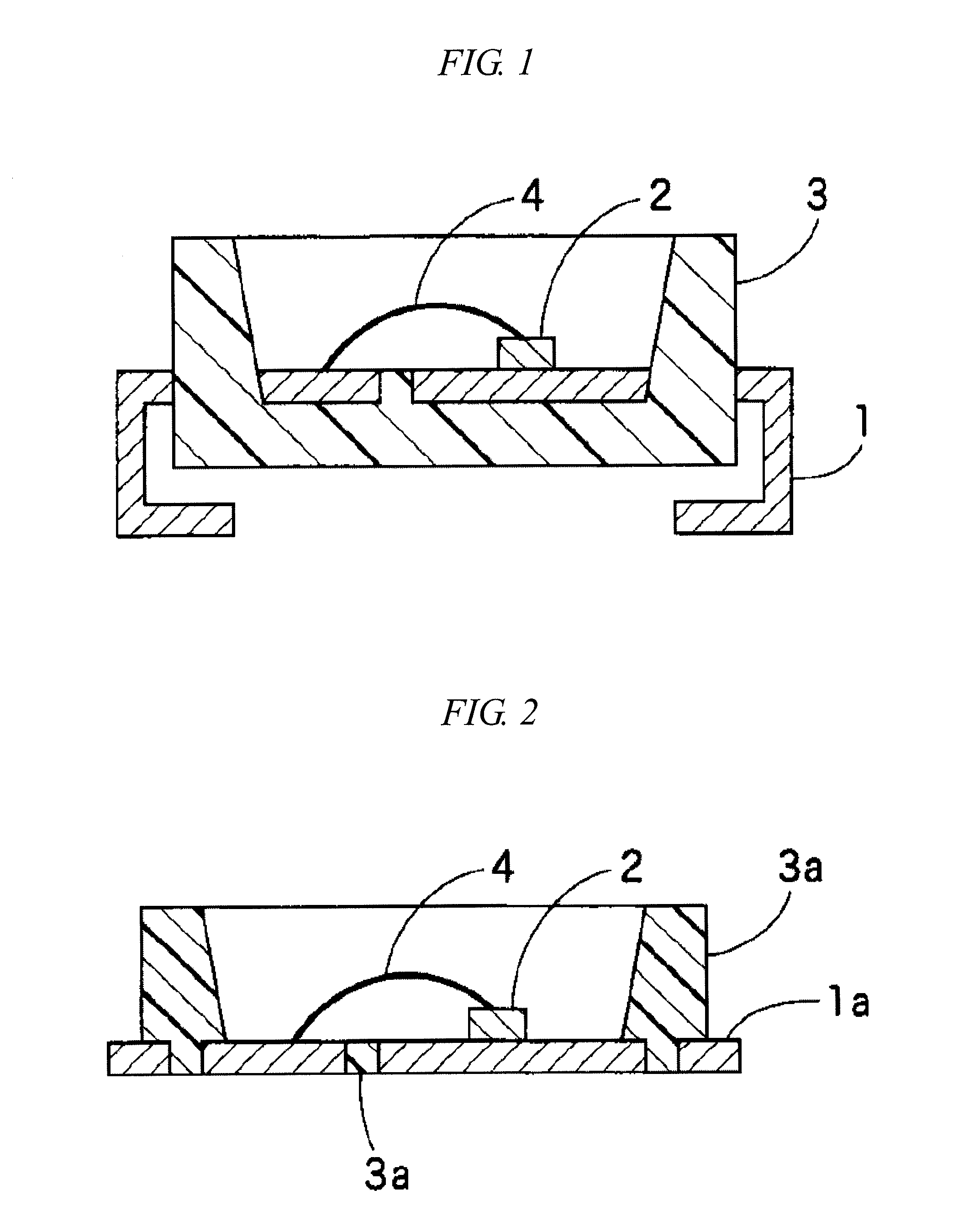
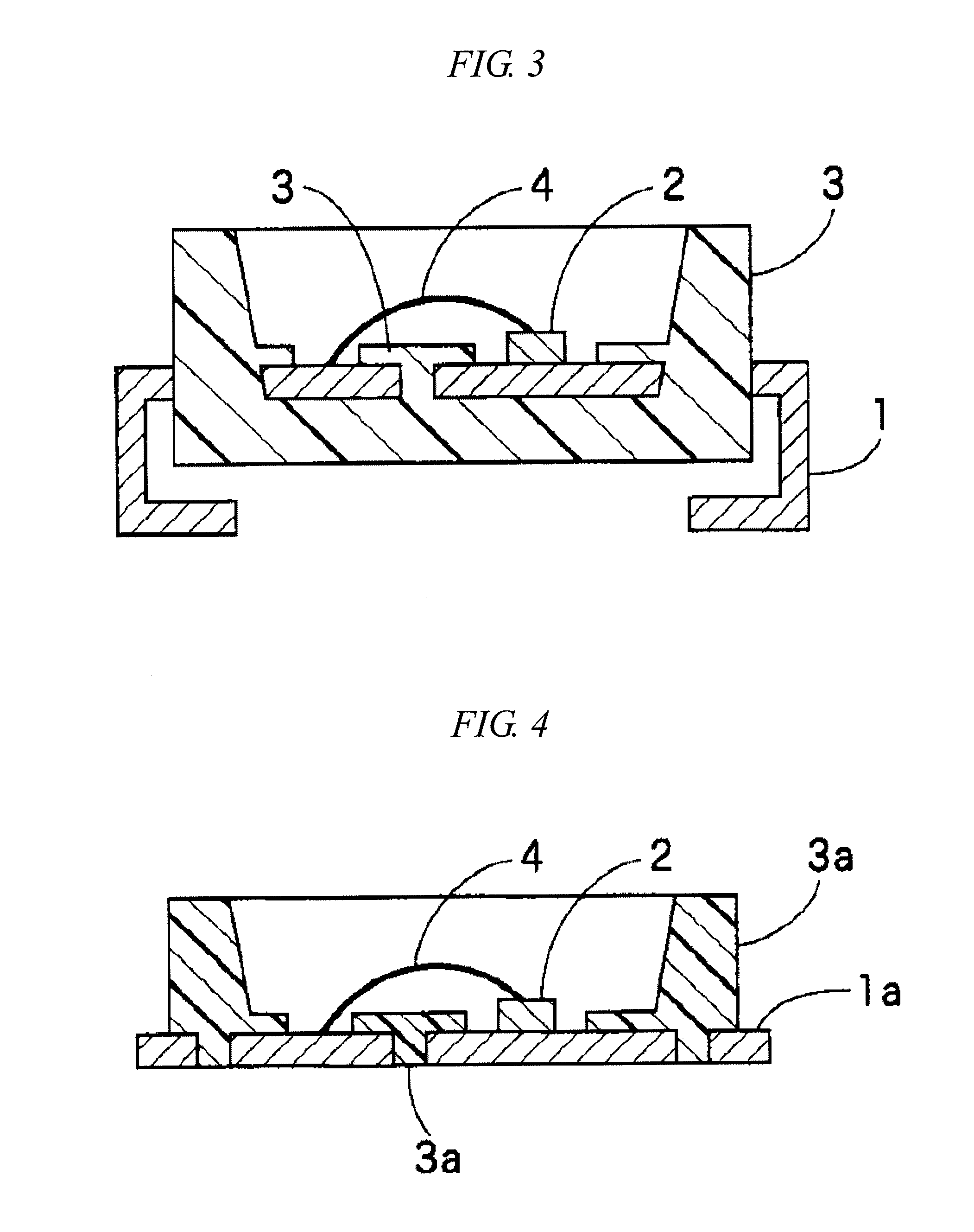
Epoxy resin composition for optical semiconductor device, lead frame for optical semiconductor device and substrate for optical semiconductor device obtained using the same, and optical semiconductor device
a technology of optical semiconductor and epoxy resin, which is applied in the direction of electrical apparatus casing/cabinet/drawer, instruments, camera filters, etc., can solve the problems of optical semiconductor device becoming remarkably brittle and optical semiconductor device becoming brittle, and achieves low linear expansion coefficient and strength, and mass-produced more inexpensively.
- Summary
- Abstract
- Description
- Claims
- Application Information
AI Technical Summary
Benefits of technology
Problems solved by technology
Method used
Image

Examples
examples
[0088]Next, Examples are given below together with Comparative Examples. However, it should not be construed that the invention is limited to these Examples.
[0089]First of all, prior to the fabrication of epoxy resin compositions, materials shown below were prepared.
[Epoxy Resin (A)]
[0090]Triglycidyl isocyanurate (epoxy equivalent: 100)
[Curing Agent (B)]
[0091]4-Methylhexahydrophthalic anhydride (acid equivalent: 168)
[White Pigment (C)]
[0092]Rutile type titanium dioxide [average particle diameter: 0.21 μm, BET specific surface area (X1): 9.0 m2 / g]
[Inorganic Filler (D)]
[0093]Spherical fused silica [average particle diameter: 22 μm, BET specific surface area (Y1): 3.2 m2 / g]
[0094]3-Glycidoxypropyl trimethoxysilane [minimum coverage area (Z1): 330 m2 / g]
[Curing Accelerator (F)]
[0095]Tetra-n-butylphosphonium-o,o-diethylphosphorodithioate
PUM
| Property | Measurement | Unit |
|---|---|---|
| wavelength range | aaaaa | aaaaa |
| light reflectivity | aaaaa | aaaaa |
| flexural elastic modulus | aaaaa | aaaaa |
Abstract
Description
Claims
Application Information