Scanning signal line drive circuit and display device provided with same

a drive circuit and signal line technology, applied in the direction of digital storage, instruments, computing, etc., can solve the problem that the source bus line cannot transmit video signals indicating pixel voltage values for more than one line at one time, and achieve the effect of improving the yield ratio, and reducing the number of circuit elements

Inactive Publication Date: 2013-02-07
SHARP KK
View PDF3 Cites 26 Cited by
  • Summary
  • Abstract
  • Description
  • Claims
  • Application Information

AI Technical Summary

Benefits of technology

[0104]According to the first aspect of the present invention, each stage of the shift register is provided with the P output nodes for outputting scanning signals. The clock signals that are different from each other are supplied as the output control clock signals to the second electrodes of the P output control switching elements whose third electrodes are respectively connected to the P output nodes. Accordingly, the P scanning signals that are sequentially driven to the ON level are outputted from each stage of the shift register. Therefore, the scanning signal lines as a whole are driven by the shift register as in the conventional example. Here, the first electrodes of the P output control switching elements are connected in common to the first-node that is turned to the ON level based on the shift pulse. Accordingly, the shift register as a whole requires a relatively small number of the circuit elements for controlling the state of the output control switching elements as compared to the conventional example. Thus, it is possible to drive the scanning signal lines as a whole as in the conventional example using a scanning signal line drive circuit configured by a relatively small number of circuit elements as compared to the conventional example. Accordingly, a yield ratio is improved as compared to the conventional example. Further, it is possible to downsize the display device.
[0105]According to the second aspect of the present invention, it is possible to reduce the number of the circuit elements that constitute the scanning signal line drive circuit without complicating the configuration of each stage of the shift register.
[0106]According to the third aspect of the present invention, the scanning signal line drive circuit capable of operating with a relatively small number of clock signals can be configured by a relatively small number of circuit elements as compared to the conventional example.
[0107]According to the fourth aspect of the present invention, during a period in which the scanning signal outputted from each stage of the shift register is to be driven to the OFF level, the output control switching elements included in the each stage are turned to the OFF state. Accordingly, it is possible to suppress an occurrence of an abnormal operation in the shift register.
[0108]According to the fifth aspect of the present invention, similarly to the fourth aspect of the present invention, it is possible to suppress an occurrence of an abnormal operation in the shift register.
[0109]According to the sixth aspect of the present invention, the scanning signal line drive circuit capable of operating with a relatively small number of clock signals can be configured by a relatively small number of circuit elements as compared to the conventional example.

Problems solved by technology

Although video signals indicating pixel voltage values are transmitted through the source bus lines, the source bus lines cannot transmit video signals indicating pixel voltage values for more than one line at one time (simultaneously).

Method used


Image

  • Scanning signal line drive circuit and display device provided with same
  • Scanning signal line drive circuit and display device provided with same
  • Scanning signal line drive circuit and display device provided with same

Examples


first embodiment

1. First Embodiment

1.1 Overall Configuration and Operation

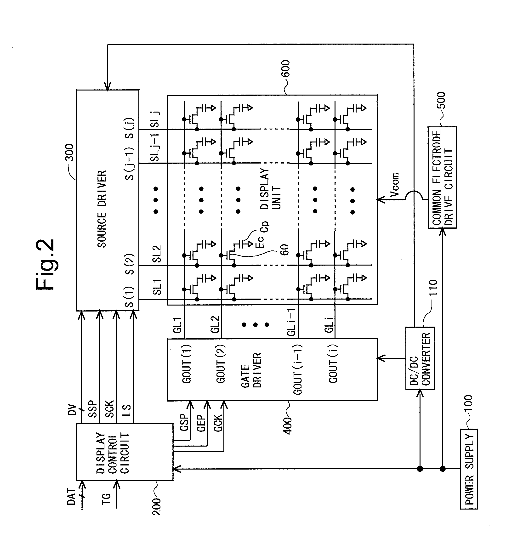
[0167]FIG. 2 is a block diagram for illustration of an overall configuration of an active matrix-type liquid crystal display device according to a first embodiment of the present invention. As illustrated in FIG. 2, this liquid crystal display device is provided with a power supply 100, a DC / DC converter 110, a display control circuit 200, a source driver (video signal line drive circuit) 300, a gate driver (scanning signal line drive circuit) 400, a common electrode drive circuit 500, and a display unit 600. Here, the gate driver 400 is formed using such as amorphous silicon, polycrystalline silicon, microcrystalline silicon, or oxide semiconductor (e.g., IGZO) on a display panel including the display unit 600. Specifically, in this embodiment, the gate driver 400 and the display unit 600 are formed on the same substrate (an array substrate that is one of two substrates that constitute a liquid crystal panel).

[0168]The displ...

second embodiment

2. Second Embodiment

2.1 Configuration of Stage Constituent Circuit

[0206]FIG. 12 is a circuit diagram showing a detailed configuration of a stage constituent circuit according to a second embodiment of the present invention. Here, an overall configuration and an operation of a liquid crystal display device and a configuration and an operation of a gate driver are the same as those in the first embodiment, and therefore descriptions for these are omitted.

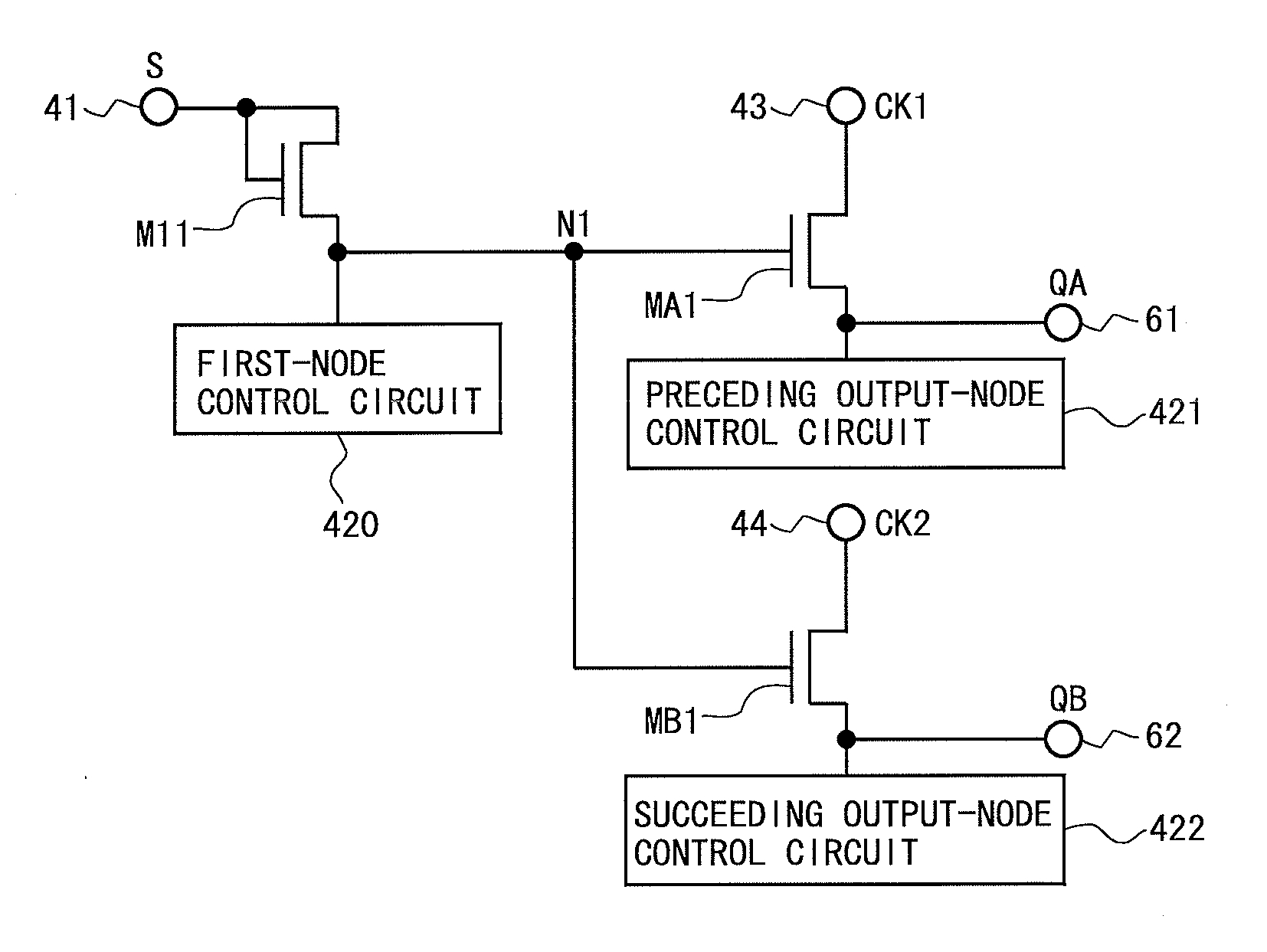
[0207]As illustrated in FIG. 12, this stage constituent circuit is provided with twelve thin-film transistors M10, M11, M12, M22, M25, M26, MA1, MA4, MA5, MB1, MB4, and MB5 and the two capacitors CA1 and CB1. Additionally, this stage constituent circuit includes the five input terminal 41-45 and the two output terminals 61 and 62, in addition to the input terminal for the low-level DC power supply potential VSS.

[0208]Next, a connecting relation among components within the stage constituent circuit is described. A drain terminal of the...

third embodiment

3. Third Embodiment

3.1 Configuration of Shift Register

[0214]FIG. 14 is a block diagram showing a configuration of a shift register 411 according to a third embodiment of the present invention. Here, an overall configuration and an operation of a liquid crystal display device are the same as those in the first embodiment, and therefore descriptions for these are omitted. Similarly to the first embodiment (see FIG. 3 and FIG. 4), the shift register 411 is configured by the z stage constituent circuits SR(1)-SR(z). Each stage constituent circuit includes an input terminal for receiving a clock signal CKA (hereinafter referred to as a “first clock”), an input terminal for receiving a clock signal CKB (hereinafter referred to as a “second clock”), an input terminal for receiving a clock signal CKC (hereinafter referred to as a “third clock”), an input terminal for receiving a clock signal CKD (hereinafter referred to as a “fourth clock”), the input terminal for receiving the low-level DC...


PUM


Abstract

A monolithic gate driver capable of operating with a relatively small number of circuit elements is realized. A stage constituent circuit constituting each stage of a shift register includes two output terminals connected to scanning signal lines, two thin-film transistors each having a drain terminal to which an output control clock signal is supplied and a source terminal connected to the output terminal, a first-node connected to the two thin-film transistors in common, a first-node control circuit, and an input terminal for receiving a set signal. In this configuration, the first-node changes from an OFF level to an ON level based on the set signal. Further, the first-node control circuit changes the first-node from the ON level to the OFF level.

Description

RELATED APPLICATIONS[0001]The present application is a National Phase of International Application No. PCT / JP2011 / 050782, filed Jan. 18, 2011, and claims priority from, Japanese Application No. 2010-118261, filed May 24, 2010.TECHNICAL FIELD[0002]The present invention relates to a display device and a drive circuit thereof, and in particular to a scanning signal line drive circuit including a shift register for driving scanning signal lines provided for a display unit of the display device.BACKGROUND ART[0003]In recent years, as for liquid crystal display devices, a gate driver (scanning signal line drive circuit) for driving gate bus lines (scanning signal lines) have become increasingly monolithic. Conventionally, a gate driver has mostly been mounted as an IC (Integrated Circuit) chip on a peripheral part of a substrate that constitutes a liquid crystal panel. However, in recent years, it has gradually become more common to provide a gate driver directly on a substrate. Such a ga...

Claims


Application Information

Patent Timeline
Patent Type & Authority Applications(United States)
IPC IPC(8): G06F3/038
CPCG09G3/20G09G3/3674G11C19/28G09G2310/0286G11C19/184G09G2310/0267
Inventor TAKAHASHI, YOSHIHISA
Owner SHARP KK
Why Eureka
Try Eureka