Nano-laminated film with transparent conductive property and water-vapor resistance function and method thereof

a technology of conductive property and water-vapor resistance, applied in the field of nano-laminated films, can solve the problems of easy damage to electronic devices, limited glass packaging method, etc., and achieve the effect of improving water vapor transmission rate, less defects, and prolonging the service life of electronic devices

Inactive Publication Date: 2013-02-21
NAT APPLIED RES LAB
View PDF1 Cites 18 Cited by
  • Summary
  • Abstract
  • Description
  • Claims
  • Application Information

AI Technical Summary

Benefits of technology

[0035](3) The atomic layer deposition (ALD) technology is used to manufacture the nano-laminated film of the present invention to produce products with less defects and better water vapor transmission rate (below 0.001 g / m2day) than those produced by the conventional methods. Since a thin film with even thickness can be formed by the present invention, therefore the required thickness is smaller than that required in the conventional manufacturing process, so that when the invention is applied to package flexible electronic devices, a thinner thin film may not be cracked easily by the bending of the flexible electronic device and the service life of the electronic device can be extended.
[0036](4) The atomic layer deposition (ALD) technology is used to manufacture the nano-laminated film of the present invention to overcome the problems of producing large-area packaging thin film in a conventional manufacturing process, so as achieve a low defective rate in the production of the large-area thin film with a low defective rate and a high performance.

Problems solved by technology

However, these electronic devices particularly OLED and OPV devices may be damaged easily when they come in contact with water vapor and oxygen in the air, and the permeability of water vapor and oxygen must be maintained at a level below 10−6 g / m2 / day and 10−5 cm3 / m2 / day respectively to prevent the devices from being damaged by water vapor and oxygen.
However, the conventional glass packaging method is restricted by the properties of glass, and the glass packaging method cannot be applied to manufacturing flexible electronic devices.
At present, if the inorganic thin film is used as the packaging thin film of the electronic devices, water vapor transmission path may be formed easily in an inorganic thin film manufacturing by the conventional manufacturing process, thus resulting in a high defective rate and a low density of the thin film.
These defects cause the flexible electronic devices are bent, small cracks are easily formed or forming a water vapor transmission path to disable the electronic device.
Therefore, the thin film requires a relatively larger thickness, and the present existing inorganic thin film packaging technologies still fail to meet the requirements of industrial applications and are limited by the high level of difficulty of manufacturing the high-performance thin film by the conventional manufacturing process, so that the area of the OLED products cannot be increased, and the high cost cannot be lowered.
Although the organic materials and composite materials used in present existing packaging technologies can meet the water vapor resisting performance requirement for industrial applications, yet the organic materials usually have a short life and indirectly affect the service life of the devices.
Similarly, if a multi-layered inorganic / organic thin film is used for manufacturing a water vapor resisting layer, both reliability and service life of the organic thin film are poor and fail to enhance the service life of the OLED products.
In addition, if chemical solutions are used for preparing the multi-layered inorganic and organic thin film to produce large-area products, the volatile solvent may cause defects of the thin film structure and the problem of a high porosity of the thin film, such that the large-area OLED products cannot be manufactured.

Method used


Image

  • Nano-laminated film with transparent conductive property and water-vapor resistance function and method thereof
  • Nano-laminated film with transparent conductive property and water-vapor resistance function and method thereof
  • Nano-laminated film with transparent conductive property and water-vapor resistance function and method thereof

Examples


Embodiment Construction

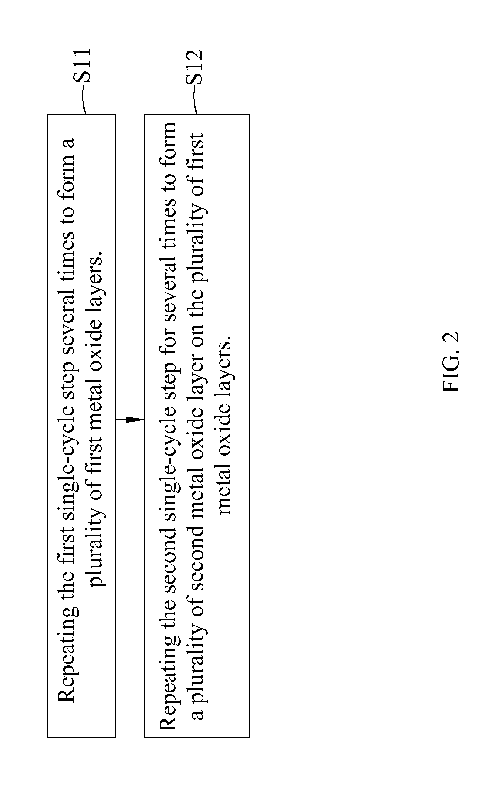
[0048]The foregoing and other objectives, technical characteristics and advantages of the present invention will become apparent with the detailed description of preferred embodiments accompanied with related drawings as follows.

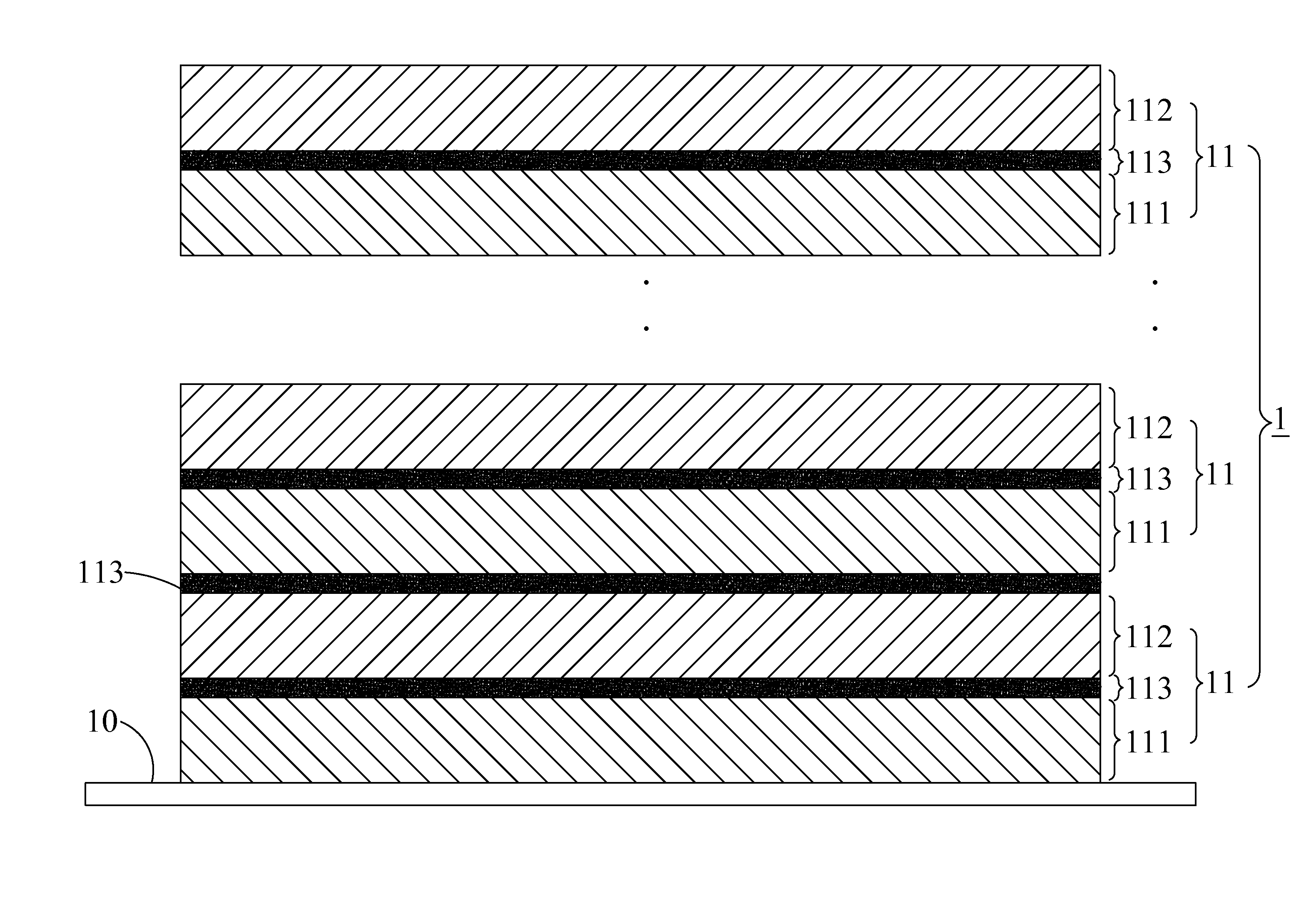
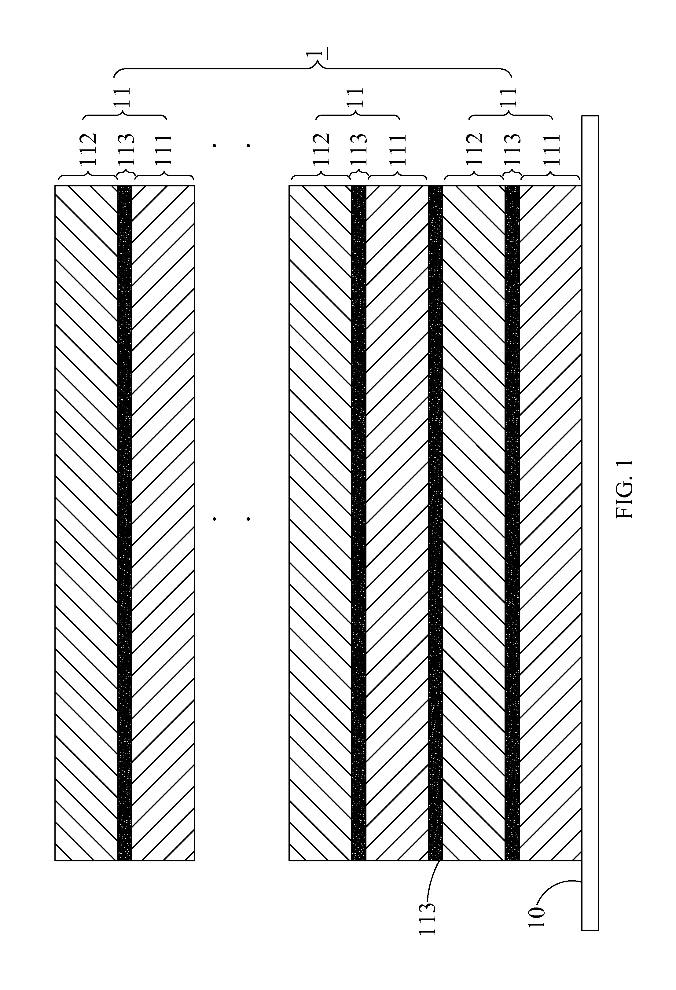
[0049]With reference to FIG. 1 for a schematic view of a nano-laminated film in accordance with a preferred embodiment of the present invention, the nano-laminated film 1 is formed on a surface of a substrate 10 of a package device, and a nanocomposite layer 11 is laminated repeatedly to achieve the packaging effect. Each nanocomposite layer 11 is comprised of a plurality of first metal oxide layers 111 and a plurality of second metal oxide layers 112, and the plurality of second metal oxide layers 112 is formed on the plurality of first metal oxide layers 111 respectively.

[0050]Wherein, a contact interface is formed between the plurality of first metal oxide layers 111 and the plurality of second metal oxide layers 112 in the structure of each nanocomposite...


PUM

PropertyMeasurementUnit
total thicknessaaaaaaaaaa
densityaaaaaaaaaa
temperatureaaaaaaaaaa

Abstract

The present invention discloses a nano-laminated film with transparent conductive property and water-vapor resistance function and method thereof. The nano-laminated film comprises a plurality of first metal oxide layers and a plurality of second metal oxide layers. Wherein, the first metal layers and the second metal layers are made of different materials, and there is a spinel phase formed between the first metal layers and the second metal layers.

Description

CROSS-REFERENCE TO RELATED APPLICATION[0001]This application claims the benefit of Taiwan Patent Application No. 100129471, filed on Aug. 17, 2011, in the Taiwan Intellectual Property Office, the disclosure of which is incorporated herein in its entirety by reference.BACKGROUND OF THE INVENTION[0002]1. Field of the Invention[0003]The present invention relates to a nano-laminated film and a manufacturing method thereof, and more particularly to the nano-laminated film with transparent conductive property and water-vapor resistance function applied in electronic products and the method thereof.[0004]2. Description of Related Art[0005]In recent years, optoelectronic products including organic light emitting diode (OLED) devices, organic photovoltaic (OPV) batteries, thin film photovoltaic batteries, flexible LCD, and the electronic paper bloom, thus playing a decisive role in present and future markets. However, these electronic devices particularly OLED and OPV devices may be damaged ...

Claims


Application Information

Patent Timeline
Patent Type & Authority Applications(United States)
IPC IPC(8): B32B9/04B05D5/12
CPCB32B19/048B32B2264/102B32B2457/206H01L51/5008H01L51/5215Y10T428/26H01L51/5256H01L2251/55H01L2251/558C23C16/45529H01L51/5234H10K30/865H10K50/816H10K50/828H10K50/8445H10K2101/00H10K2102/351
Inventor YU, CHIH-CHIEHTSAI, MENG-YENKEI, CHI-CHUNGLIU, BO-HENGHSIAO, CHIEN-NAN
Owner NAT APPLIED RES LAB
Why Eureka
Try Eureka