Variation Resistant Metal-Oxide-Semiconductor Field Effect Transistor (MOSFET)

Active Publication Date: 2013-02-28
SEMIWISE
View PDF4 Cites 31 Cited by
  • Summary
  • Abstract
  • Description
  • Claims
  • Application Information

AI Technical Summary

Benefits of technology

[0028]FIG. 3E is a diagram showing a slab doping profile, which might be realized either by low temperature, doped epitaxy or by at

Problems solved by technology

It is well-known in the art that as MOSFETs move to finer and finer dimensions, variability of the threshold voltage σVT seriously undermines the reproducibility of threshold voltages among otherwise identical transistors.
This effect is inevitable, and it is particularly severe in its impact on complimentary MOS (CMOS) static random access memories (SRAM), which use millions of near-minimum sized transistors.
This trend moves away from the more traditional bulk MOS manufacturing, adversely impacting costs and availability.
However, this is an exceedingly

Method used


Image

  • Variation Resistant Metal-Oxide-Semiconductor Field Effect Transistor (MOSFET)
  • Variation Resistant Metal-Oxide-Semiconductor Field Effect Transistor (MOSFET)
  • Variation Resistant Metal-Oxide-Semiconductor Field Effect Transistor (MOSFET)

Examples


Embodiment Construction

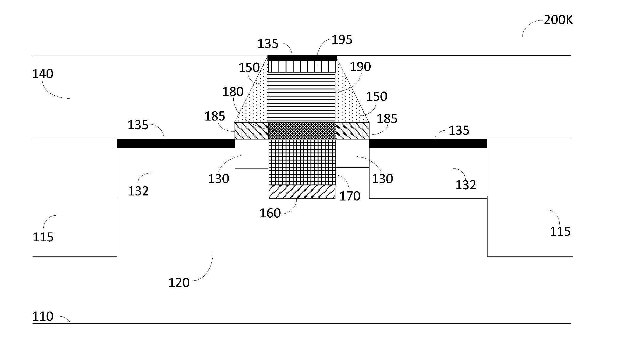
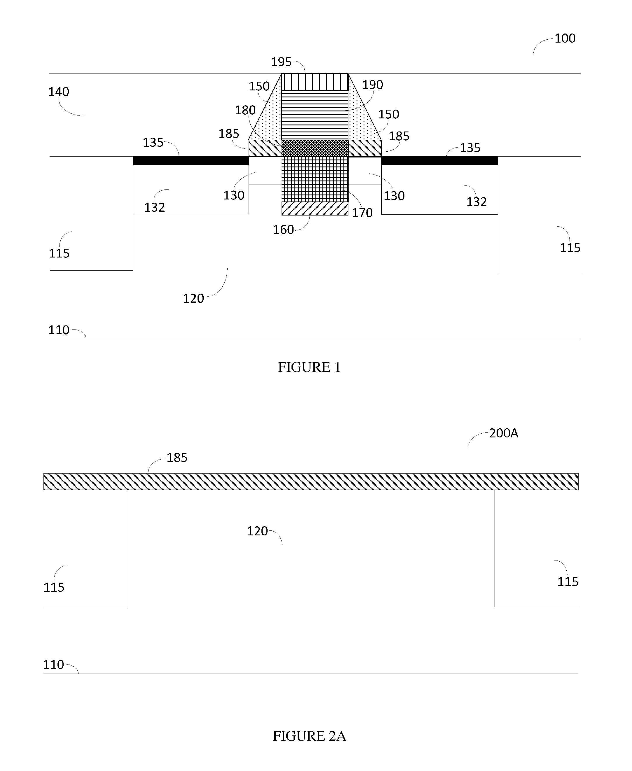
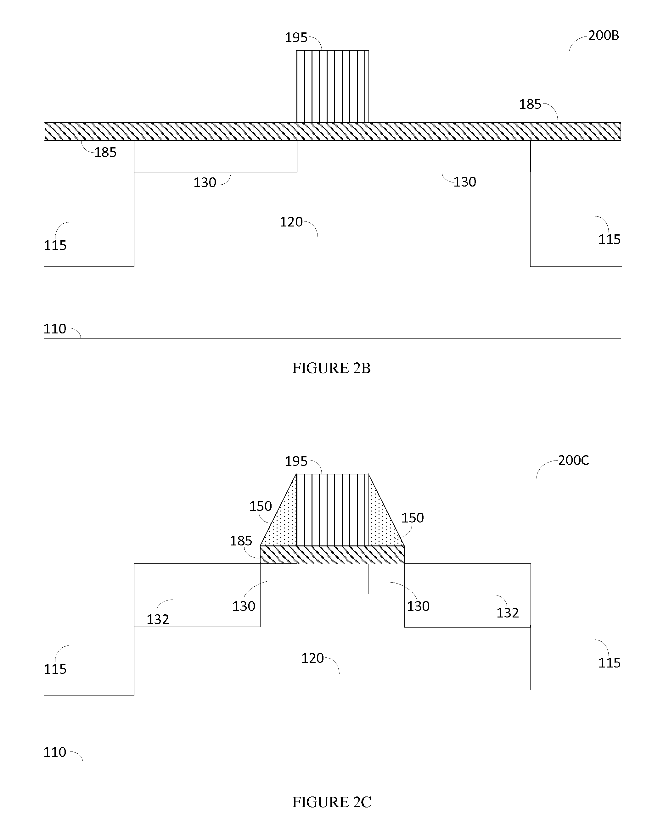
[0033]Variation resistant metal-oxide-semiconductor field effect transistors (MOSFETs) are manufactured using a high-K, metal, ‘channel-last’ process. Between spacers formed over a well area having separate drain and source areas, a cavity and then a recess into the well area are formed. The active region is formed on top of an optional thin highly doped layer over which an un-doped or lightly doped epitaxial layer is formed. The high doping beneath the low doped epitaxial layer can be achieved utilizing low-temperature epitaxial growth (not to exceed 750° C. but preferably not exceeding 650° C.) with single or multiple delta doping, or slab doping. This epitaxial growth may be effected using conventional low-temperature epitaxy, molecular beam epitaxy or atomic layer deposition. A high-K dielectric stack is formed over the upper or epitaxial layer over which a metal gate is formed within the cavity boundaries. In one embodiment of the invention a cap of poly-silicon or amorphous si...


PUM


Abstract

Variation resistant metal-oxide-semiconductor field effect transistors (MOSFETs) are manufactured using a high-K, metal-gate ‘channel-last’ process. A cavity is formed between spacers formed over a well area having separate drain and source areas, and then a recess into the well area is formed. The active region is formed in the recess, comprising an optional narrow highly doped layer, essentially a buried epitaxial layer, over which a second un-doped or lightly doped layer is formed which is a channel epitaxial layer. The high doping beneath the low doped epitaxial layer can be achieved utilizing low-temperature epitaxial growth with single or multiple delta doping, or slab doping. A high-K dielectric stack is formed over the channel epitaxial layer, over which a metal gate is formed within the cavity boundaries. In one embodiment of the invention a cap of poly-silicon or amorphous silicon is added on top of the metal gate.

Description

CROSS-REFERENCE TO RELATED APPLICATIONS[0001]This application claims the benefit of U.S. Provisional Patent Application No. 61 / 256,033 filed Aug. 22, 2011 and U.S. Provisional Patent Application No. 61 / 568,523 filed Dec. 8, 2011.BACKGROUND OF THE INVENTION[0002]1. Field of the Invention[0003]The present invention generally relates to the manufacturing of metal-oxide-semiconductor field effect transistors (MOSFETs), and more particularly to MOSFETs manufactured for reproducibility of threshold voltages among otherwise identical transistors.[0004]2. Prior Art[0005]Random variation in threshold voltage (σVT) of metal-oxide semiconductor (MOS) field effect transistors (MOSFETs) with high-K (high dielectric constant) metal gate stack is caused by some dominant factors: (i) random dopant fluctuations (RDF) in the well and in the pocket implant regions underneath the gate, which, among other things, cause variations in depletion layer thickness; (ii) line edge roughness (LER) which causes ...

Claims


Application Information

Patent Timeline
IPC IPC(8): H01L29/78H01L21/336
CPCH01L29/517H01L29/665H01L29/66545H01L29/105H01L29/66651H01L29/7833H01L29/6659H01L21/02164H01L21/0262H01L21/02631H01L21/02636H01L21/30604H01L21/31053H01L21/31111H01L21/823437H01L29/365H01L29/6656
Inventor ASENOV, ASENROY, GARETH
Owner SEMIWISE
Why Eureka
Try Eureka