
Eureka
For R&D, Eureka makes reading and utilizing patents & technical documents easy.
Eureka AIR
Designed for self-driven R&D workflows. Generate viable solutions, solve complex R&D challenges, empower your innovation with AI.

Eureka Materials
Designed for material experts only. Revolutionize your material R&D, from search, analyze, to developing new materials.

TechResearch
Generate reliable direction feasibility study reports for your R&D in just a few steps.

TechSeek
Discover and master advanced knowledge NOW. Basics, ideas, possibilities, all at once.

TechMind
As an expert in R&D Theories, TechMind can generates customized viable solutions instantly.

TechRisk
Analyze your overall solution with one click, know your potential R&D risks in advance.

TechMonitor
Get weekly tech updates, stay abreast of the latest tech innovations and key insights.
Optical device, optical module, and method for manufacturing optical device
- Summary
- Abstract
- Description
- Claims
- Application Information
AI Technical Summary
Benefits of technology
Problems solved by technology
Method used
Image

Examples
first embodiment
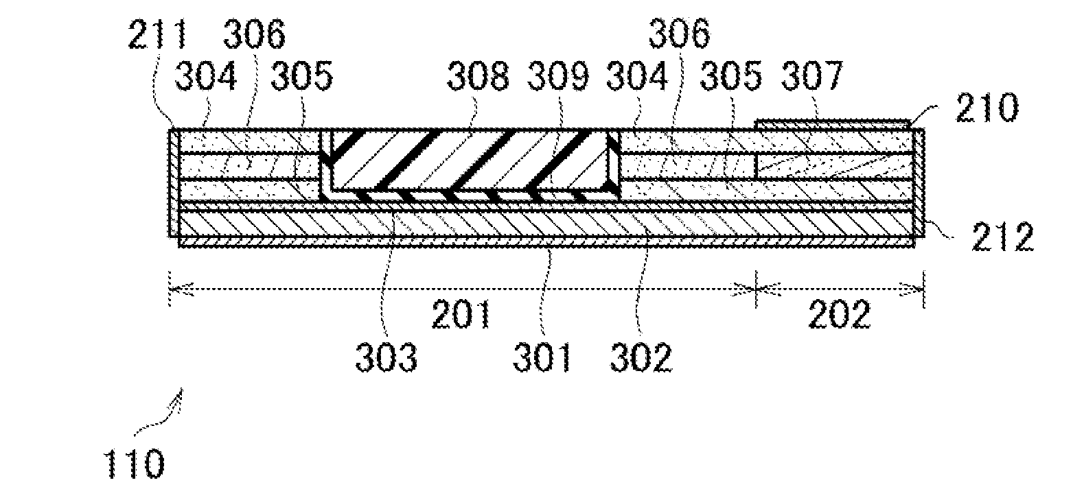
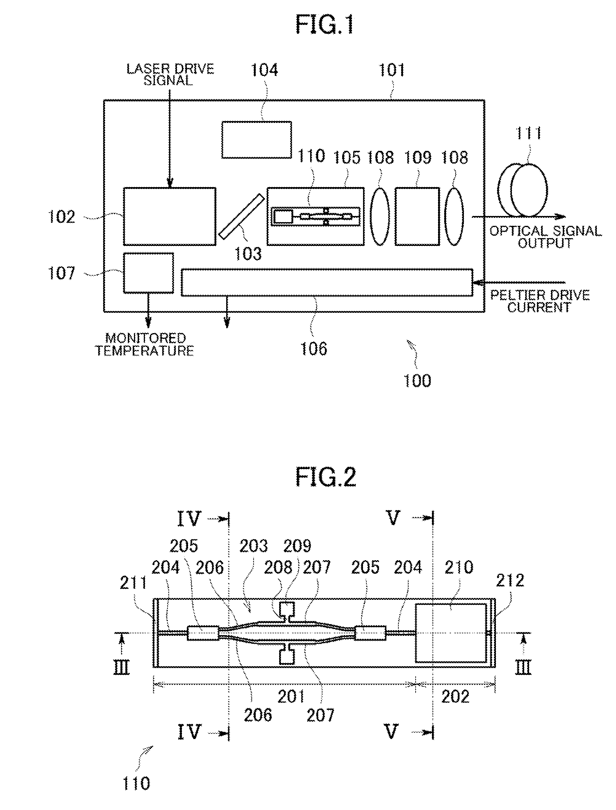
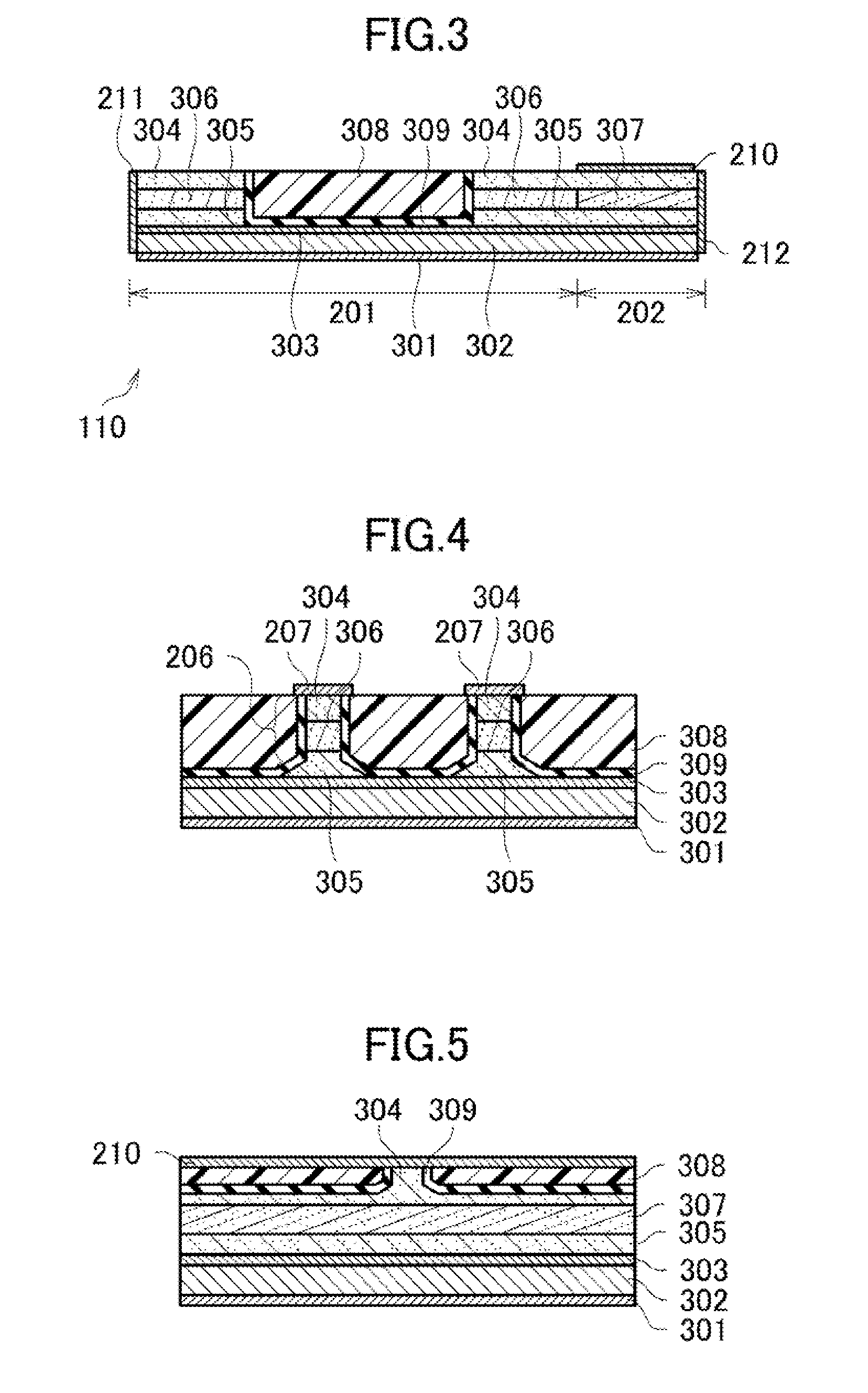
[0055]FIG. 1 is a diagram illustrating an overall configuration of an optical module according to a first embodiment of the present invention. As illustrated in FIG. 1, an optical module 100 includes, in a package 101, a tunable laser 102, a half mirror 103, a wavelength locker 104, a carrier 105, a Peltier 106, a thermistor 107, a plurality of condenser lenses 108, and an optical isolator 109.
[0056]The carrier 105 is provided with a terminator (not shown), and incorporates an optical device 110 including a semiconductor Mach-Zehnder modulator. The package 101 is formed by processing a metal material into a box shape. For example, the package 101 includes a baseplate made of a CuW alloy having high thermal conductivity, a frame made of a FeNi alloy, a ceramic feedthrough on which a wiring pattern for transmitting an electrical signal to the inside of the package 101 is formed, a lead terminal, a seam ring for seam-welding a cap, sapphire glass for hermetically sealing a window throu...
second embodiment
[0105]Next, a second embodiment of the present invention is described. An optical device 810 in this embodiment is different from the optical device in the first embodiment mainly in that a laser 811, the semiconductor optical modulator 202, and the semiconductor Mach-Zehnder modulator 201 are integrated. A method of manufacturing the optical device 810 in this embodiment is different from the method of manufacturing an optical device in the first embodiment mainly in that only dry etching is used for forming the high mesa of the semiconductor Mach-Zehnder modulator 201. In the following, description of the same parts as in the first embodiment is omitted.
[0106]FIG. 9 schematically illustrates a top surface of the optical device according to this embodiment. FIG. 10 schematically illustrates a cross-section taken along the line X-X of FIG. 9. FIG. 11 schematically illustrates a cross-section taken along the line XI-XI of FIG. 9. FIG. 12 schematically illustrates a cross-section take...
third embodiment
[0122]Next, a third embodiment of the present invention is described. An optical device 120 in this embodiment is different from the optical device in the first embodiment mainly in that a semiconductor Mach-Zehnder modulator 201 having a high-mesa optical waveguide structure and a semiconductor laser 122 having a low-mesa optical waveguide structure are monolithically-integrated and that a low-mesa etch stop layer 132 is independently formed. In the following, description of the same parts as in the first embodiment is omitted.
[0123]FIG. 13 schematically illustrates atop surface of the optical device according to this embodiment. FIG. 14 schematically illustrates a cross-section taken along the line XIV-XIV of the optical device illustrated in FIG. 13. FIG. 15 schematically illustrates a cross-section taken along the line XV-XV of the optical device illustrated in FIG. 13. FIG. 16 schematically illustrates a cross-section taken along the line XVI-XVI of the optical device illustrat...
PUM
 Abstract
Description
Claims
Application Information
 - R&D Engineer
- R&D Manager
- IP Professional
- Industry Leading Data Capabilities
- Powerful AI technology
- Patent DNA Extraction
Browse by: Latest US Patents, China's latest patents, Technical Efficacy Thesaurus, Application Domain, Technology Topic, Popular Technical Reports.
© 2024 PatSnap. All rights reserved.Legal|Privacy policy|Modern Slavery Act Transparency Statement|Sitemap|About US| Contact US: help@patsnap.com