Resist pattern forming method, resist pattern, positive resist composition, nanoimprint mold and photomask

a technology of resist pattern and composition, which is applied in the field of resist pattern forming method, resist pattern, positive resist composition, nanoimprint mold and photomask, can solve the problems of unsatisfactory resolution performance of ultrafine pattern and good nanoedge roughness at present, and achieve high resolution, high sensitivity, and high resolution.

Active Publication Date: 2013-02-28
FUJIFILM CORP
View PDF2 Cites 2 Cited by
  • Summary
  • Abstract
  • Description
  • Claims
  • Application Information

AI Technical Summary

Benefits of technology

[0012]An object of the present invention is to provide a resist pattern forming method capable of, even in the formation of an ultrafine (for example, a 1:1 line-and-space with a line width of 30 nm or less) pattern, forming a pattern satisfying high sensitivity, high resolution property (for example, high resolution and small line edge roughness (LER)) and excellent pattern profile all at the same time, a resist pattern, a positive resist composition, a nanoimprint mold and a photomask.
[0013]As a result of intensive studies, the present inventors have found that when a film with a specific thickness formed using a positive resist composition containing a polymer compound having a specific structure is patternwise exposed and then developed by using an alkali developer having a specific alkali component concentration, the above-described object can be attained.

Problems solved by technology

However, for example, the resolution performance for an ultrafine pattern and good nanoedge roughness are not satisfied at present by any of the combinations of a resist composition and the like disclosed.

Method used


Image

  • Resist pattern forming method, resist pattern, positive resist composition, nanoimprint mold and photomask
  • Resist pattern forming method, resist pattern, positive resist composition, nanoimprint mold and photomask
  • Resist pattern forming method, resist pattern, positive resist composition, nanoimprint mold and photomask

Examples


synthesis example 1

Synthesis of Polymer Compound (R-11)

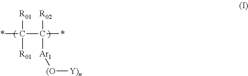
[0259]Poly(p-hydroxystyrene) (VP-2500, produced by Nippon Soda Co., Ltd.) (30 g) as a polyhydroxystyrene compound was dissolved in 120 g of PGMEA (propylene glycol monomethyl ether acetate). To this solution, 10.40 g of 2-cyclohexylethyl vinyl ether as a vinyl ether compound and 1.45 g of 2 mass % comphorsulfonic acid (PGMEA solution) were added thereto, and the mixture was stirred at room temperature for 2 hours. Furthermore, 1.05 g of 10 mass % triethylamine (PGMEA solution) was added and after stirring for a while, the reaction solution was transferred to a separating funnel containing 165 mL of ethyl acetate. The organic layer was washed with 200 mL of distilled water three times, and ethyl acetate was removed in an evaporator. The obtained reaction solution was added dropwise to 2 L of hexane, and the supernatant was removed. The obtained product was dissolved in 95 g of PGMEA, and the low-boiling-point solvent was removed under reduced press...


PUM

PropertyMeasurementUnit
thicknessaaaaaaaaaa
widthaaaaaaaaaa
thicknessaaaaaaaaaa

Abstract

A resist pattern forming method includes: in the following order, (1) a step of forming a film on a substrate by using a positive resist composition; (2) a step of exposing the film; and (4) a step of performing development by using an alkali developer after the exposing, wherein the positive resist composition contains (A) a polymer compound having a repeating unit represented by the following formula (I) as defined in the specification, a thickness of the film formed in the step (1) is from 15 to 40 nm, and an alkali component concentration in the alkali developer is from 0.5 to 1.1 mass %.

Description

BACKGROUND OF THE INVENTION[0001]1. Field of the Invention[0002]The present invention relates to a resist pattern forming method suitably usable in the ultramicrolithography process such as production of VLSI or a high-capacity microchip as well as in other photofabrication processes and capable of forming a highly defined pattern by using an electron beam (EB) or an extreme-ultraviolet ray (EUV), a resist pattern, a positive resist composition, a nanoimprint mold and a photomask. More specifically, the present invention relates to a resist pattern forming method for use in the process where a substrate with a specific underlying film is used, a resist pattern, a positive resist composition, a nanoimprint mold and a photomask.[0003]The resist pattern forming method of the present invention can be also suitably used for the production method of a nanoimprint mold structure.[0004]2. Description of the Related Art[0005]In the microfabrication using a resist composition, with an increas...

Claims


Application Information

Patent Timeline
Patent Type & Authority Applications(United States)
IPC IPC(8): G03F7/20G03F1/00B32B3/10B29C59/02C08F257/00B82Y40/00
CPCG03F1/68G03F7/0002B82Y40/00G03F7/0392Y10T428/24802G03F7/405G03F7/0397B82Y10/00C08F8/14C08F212/14C08F212/24G03F1/22G03F7/0045G03F7/26C08F212/22
Inventor TSUCHIHASHI, TORUSHIBATA, MICHIHIRO
Owner FUJIFILM CORP
Why Eureka
Try Eureka