High-frequency power amplifying device

Active Publication Date: 2013-03-07
RENESAS ELECTRONICS CORP
View PDF4 Cites 29 Cited by
  • Summary
  • Abstract
  • Description
  • Claims
  • Application Information

AI Technical Summary

Benefits of technology

[0016]With such a configuration, when the first differential amplifier is in the non-operating state, the differential transistor pair is off and through-feed current does not flow, so that the first secondary coil can be equivalently almost short-circuited. In this case as well, the influence exerted by the capacitance in the differential transistor pair which is off on another differen

Problems solved by technology

As a result, the some impedance disturbs impedance matching between the differential amplifier which is in the operating state and a load (R1 in FIG. 1), so that the efficiency of transmitting output power of the power amplifier may deteriorate.
To prevent the deterioration, there is the possibility that the circuit configuration of the power amplifier may be complicated.
In particular, in the case of setting a differential amplifier for the high-power mode to the

Method used


Image

  • High-frequency power amplifying device
  • High-frequency power amplifying device
  • High-frequency power amplifying device

Examples


first embodiment

Basic Configuration (Type 1) of Main Part of High-Frequency Power Amplifying Device

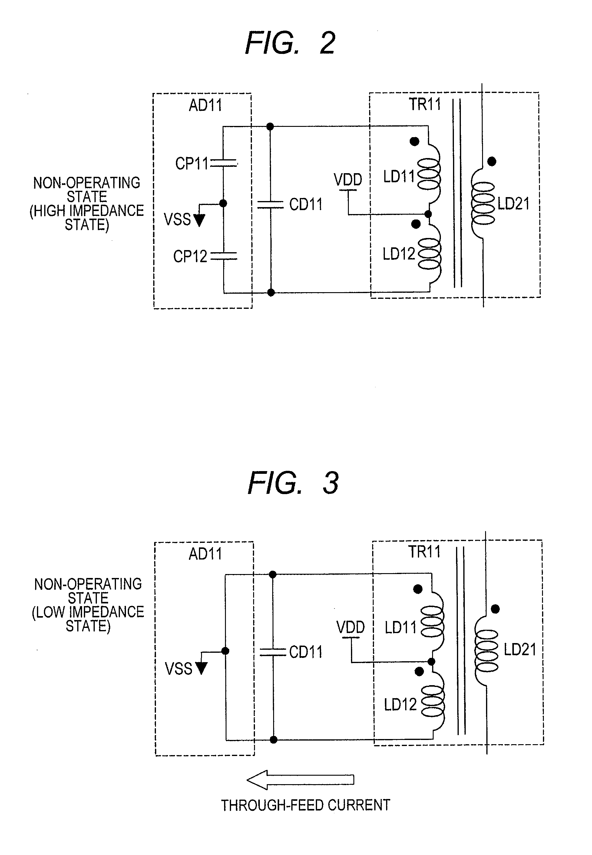
[0057]FIG. 4 is a circuit diagram showing an example of a differential amplifier in a high-frequency power amplifying device according to a first embodiment of the invention, which is controlled in a non-operating state and an equivalent circuit including a transformer corresponding to the differential amplifier. FIG. 4 shows a differential amplifier AD1, a transformer TR1, and a capacitance CD1 for impedance adjustment and, in addition, an impedance correction block MBK1. The differential amplifier AD1 is constructed by, for example, a pair of differential MOSFETs (not shown) and the MOSFETs are turned off in the non-operating state. In this case, the differential amplifier AD1 is equivalently expressed by source-drain parasitic capacitances CP1 and CP2 of the MOSFETs as a differential pair. One ends of the parasite capacitances CP1 and CP2 (the source side of the MOSFETs) are commonly coupled to a g...

second embodiment

1. Circuit Configuration and Operation of High-Frequency Power Amplifying Device in Plural Power Modes (Type 1)

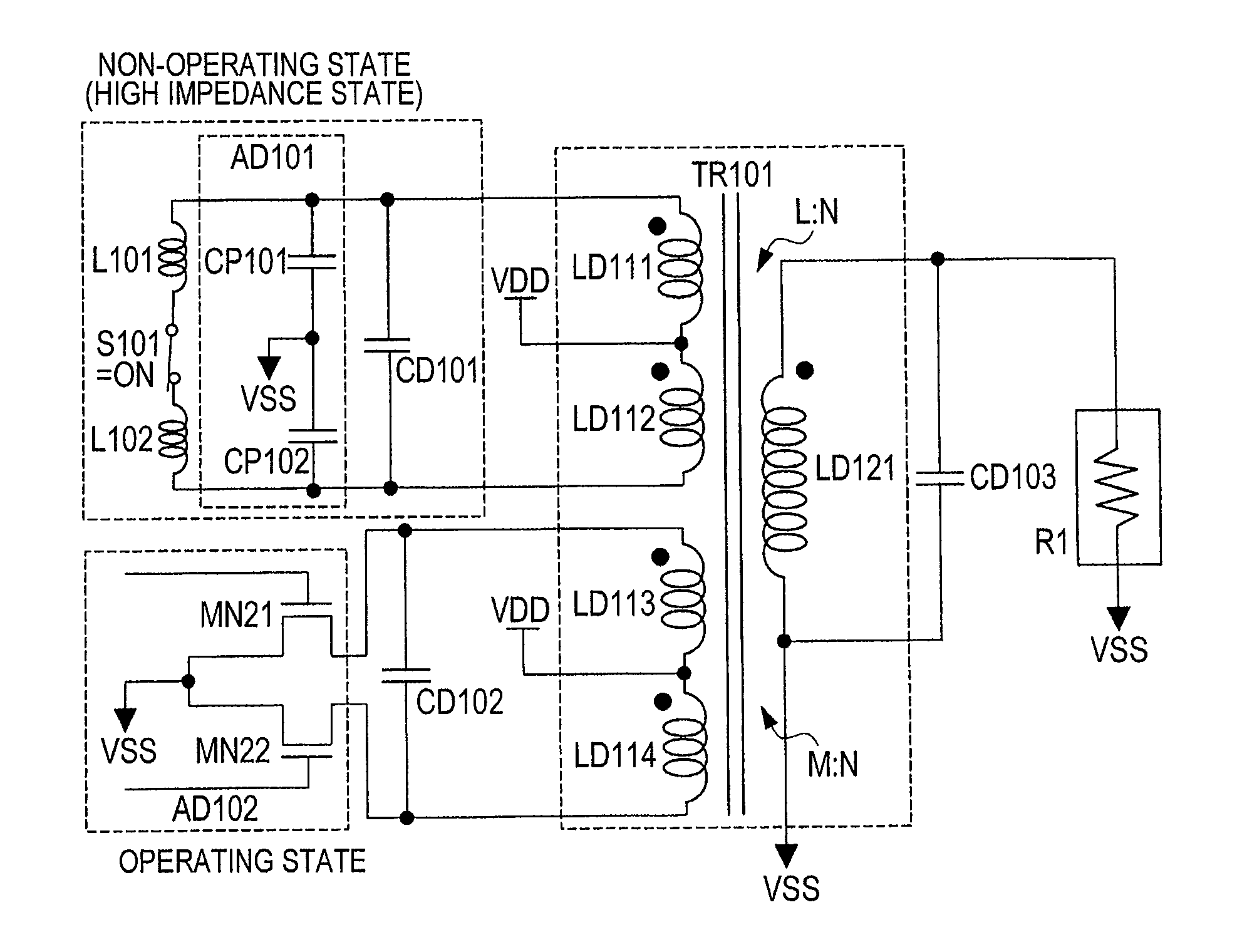
[0074]FIG. 7 is a circuit diagram showing an example of the configuration of a high-frequency power amplifying device according to a second embodiment of the invention. The high-frequency power amplifying device shown in FIG. 7 has two differential amplifiers AD101 and AD102 and a transformer TR101 having two primary coils and one secondary coil. One of the two primary coils of TR101 is constructed by two coils LD111 and LD112, and the other primary coil is also constructed by two coils LD113 and LD114. LD111 is coupled in series to LD112 via a center tap, and LD113 is coupled in series to LD114 via a center tap. To the center tap, the power supply voltage VDD is supplied.

[0075]The two primary coils of TR101 are magnetically coupled to the common secondary coil LD121 of TR101. The gate width (or emitter area) of a transistor as a component of the differential amplifier AD10...

third embodiment

1. Circuit Configuration and Operation of High-Frequency Power Amplifying Device in Plural Power Modes (Type 2[1])

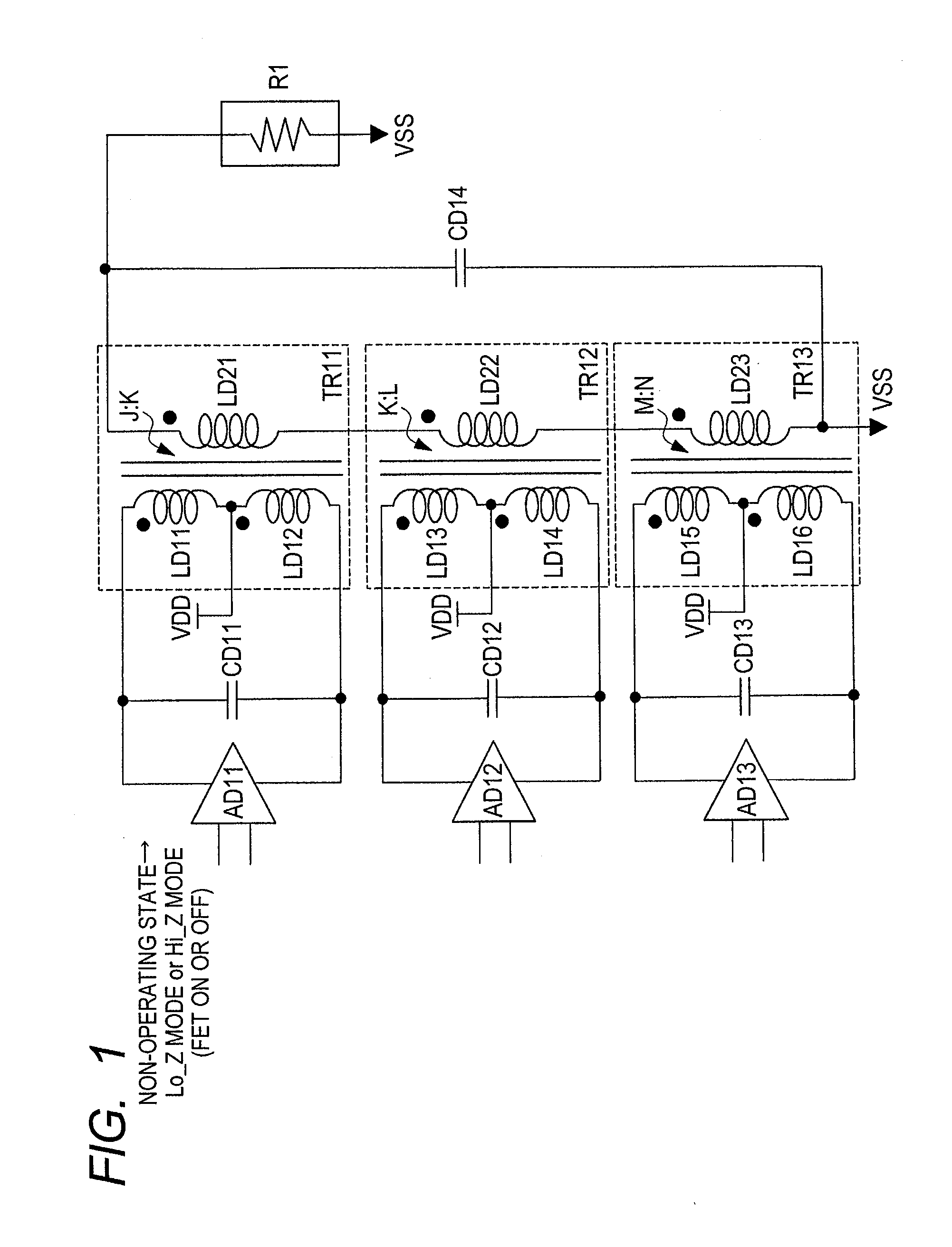
[0089]FIG. 12 is a circuit diagram showing an example of the configuration of a high-frequency power amplifying device according to a third embodiment of the invention. The high-frequency power amplifying device shown in FIG. 12 has two differential amplifiers AD201 and AD202 and two transformers TR201 and TR202. A primary coil of TR201 has a configuration that two coils LD211 and LD212 are coupled in series via a center tap. Similarly, a primary coil of TR202 has a configuration that two coils LD213 and LD214 which are coupled in series via a center tap. To the center tap, the power supply voltage VDD is supplied.

[0090]Differential outputs of AD201 are coupled to the primary coils LD211 and LD212 of the transformer TR201 and, further, magnetically coupled to a secondary coil LD221 of TR201. Differential outputs of AD202 are coupled to the primary coils LD213 and LD214 o...


PUM


Abstract

The present invention provides a high-frequency power amplifying device capable of transmitting output power at high efficiency. For example, a high-frequency power amplifying device has first and second differential amplifiers and a transformer for matching output impedances of the differential amplifiers. Between differential output nodes of the first differential amplifier, an inductor, a switch, and an inductor are coupled in series. When the second differential amplifier is in an operating state and the first differential amplifier is in a non-operating state, the switch is controlled to be on. In this case, due to “off capacitance” in transistors of a differential pair included in the first differential amplifier, impedance on the first differential amplifier side seen from both ends of primary coils becomes a high impedance state (parallel resonance state) and, equivalently, the primary coils do not exert influence on the operation of the second differential amplifier.

Description

CROSS-REFERENCE TO RELATED APPLICATIONS[0001]The disclosure of Japanese Patent Application No. 2011-193675 filed on Sep. 6, 2011 including the specification, drawings and abstract is incorporated herein by reference in its entirety.BACKGROUND[0002]The present invention relates to a high-frequency power amplifying device and, more particularly, to a technique effectively applied to a high-frequency power amplifying device used for a transmitter of a cellular phone.[0003]For example, Patent Literature 1 discloses a configuration having an amplifier for a high-output mode, an amplifier for an intermediate-output mode, an amplifier for a low-output mode, and a transformer for combining outputs of the amplifiers. For example, in operation in the high-output mode, the amplifier for the intermediate-output mode and the amplifier for the low-output mode are controlled in a high-impedance state or a low-impedance state.RELATED ART LITERATUREPatent Literature[0004]U.S. Pat. No. 7,728,661SUMMA...

Claims


Application Information

Patent Timeline
IPC IPC(8): H03F3/45H03F3/68
CPCH03F1/0277H03F3/211H03F2200/541H03F3/72H03F2200/537H03F3/245H03H7/38H03H7/09
Inventor KONDO, MASAO
Owner RENESAS ELECTRONICS CORP
Why Eureka
Try Eureka