Method of Screening Static Random Access Memory Cells for Positive Bias Temperature Instability

a random access memory and temperature instability technology, applied in static storage, information storage, digital storage, etc., can solve the problems of increasing the probability of read and write functional failure, physical scaling of device size raises significant issues, and increases the variability of electrical characteristics, so as to improve the screen conditions

Active Publication Date: 2013-03-07
TEXAS INSTR INC
View PDF4 Cites 18 Cited by
  • Summary
  • Abstract
  • Description
  • Claims
  • Application Information

AI Technical Summary

Benefits of technology

[0025]Embodiments of this invention provide such a memory and method that are capable of accurately and efficiently identifying such susceptible memory cells so as to minimize unnecessary yield loss.
[0026]Embodiments of this invention provide such a memory and method that can be readily implemented into modern manufacturing technology without requiring a precision photolithography operation.
[0027]Embodiments of this invention provide such a memory and method that can incorporate threshold voltage temperature dependence into the screen, avoiding the need to test the memories at temperature.
[0031]In some embodiments, the n-channel MOS transistors in a given SRAM cell are constructed in p-wells that are isolated from one another to allow asymmetric body node bias during the functional test, to further improve the screen conditions. For example, in one embodiment, the driver transistors are constructed in p-wells that are isolated from that of their associated n-channel pass transistors.

Problems solved by technology

However, this physical scaling of device sizes raises significant issues, especially in connection with embedded SRAM but also in SRAM realized as “stand-alone” memory integrated circuit devices.
Several of these issues are due to increased variability in the electrical characteristics of transistors formed at these extremely small feature sizes.
This variability in characteristics has been observed to increase the likelihood of read and write functional failures, on a cell-to-cell basis.
The combination of increased device variability with the larger number of memory cells (and thus transistors) within an integrated circuit renders a high likelihood that one or more cells cannot be read or written as expected.
As mentioned above, device variability and other factors can cause read and write failures, particularly in memory cells constructed with sub-micron minimum feature size transistors.
A write failure occurs when an addressed SRAM cell does not change its stored state when written with the opposite data state.
Typically, this failure has been observed to be due to the inability of write circuitry to pull down the storage node currently latched to a high voltage.
One cause of a write failure is weakness in the drive of a pass transistors (transistors 5a, 5b of cell 2).
The apparent trip voltage Vtrip at bit line BLBk that actually causes a successful write will thus be lower than optimal, due to the weakness of pass transistor 5b. It has been observed that write failures (i.e., the measure Vtrip) has a worst case at low temperature.
Cell stability failures are the converse of write failures—while a write failure occurs if a cell is too stubborn in changing its state, a cell stability failure occurs if a cell changes its state too easily during a read.
A cell stability failure also occurs if a write to a selected memory cell causes a false write of data to unselected cells in that same row (i.e., to the “half-selected” cells in unselected columns of the selected row).
The possibility of such stability failures is exacerbated by device mismatch and variability, as discussed above.
As known in the art, it is becoming increasingly difficult to design the appropriate test “vectors” (i.e., combinations of bias and internal circuit voltages, and other test conditions) that identify devices that are vulnerable to failure over time and temperature, without significant yield loss of devices that would not fail over operating life yet fail the screen at the applied guardbanded test vectors.
This difficulty is exacerbated by transistor degradation mechanisms that have become observable at the extremely small minimum feature sizes in modern integrated circuits.
In the context of CMOS SRAMs, NBTI degradation affects the ability of memory cells to store and retain data.
It has been observed, however, that degradation due to PBTI of n-channel transistors with silicon dioxide gate dielectrics is very slight, especially as compared to the NBTI degradation of p-channel transistors in the same circuits.
It has been observed, however, that high-k metal gate n-channel MOS transistors are vulnerable to threshold voltage shifts due to PBTI, even though their conventional gate dielectric n-channel devices are not.
This vulnerability is believed due to the affinity of HfO2 films to trap electrons under positive gate bias (relative to the transistor channel region).
And PBTI degradation of the n-channel cell transistors can cause read current failures in read cycles, in which weakened read current causes an insufficient differential signal to be developed across bit lines and results in an incorrect data state being read.
To the extent that potential proxies for this effect are available, modern reliability goals may require an excessively harsh screen margin (e.g., guardband voltages above the maximum operating voltages) that itself may degrade long-term reliability.
In addition, the undue yield loss of devices that fail such a screen but would, in fact, not have degraded to failure, can be substantial.
The increased load transistor drive during write will tend to cause write failures for those cells having a pass transistor with weakened drive due to a bit line side defect.

Method used


Image

  • Method of Screening Static Random Access Memory Cells for Positive Bias Temperature Instability
  • Method of Screening Static Random Access Memory Cells for Positive Bias Temperature Instability
  • Method of Screening Static Random Access Memory Cells for Positive Bias Temperature Instability

Examples


Embodiment Construction

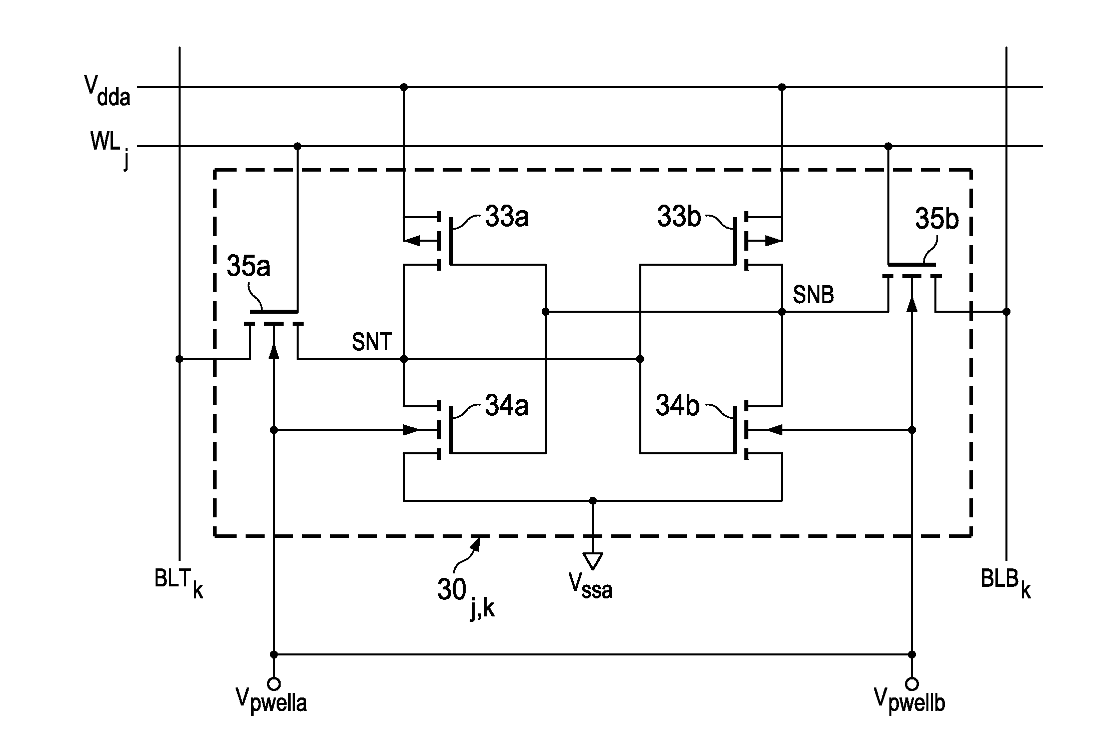
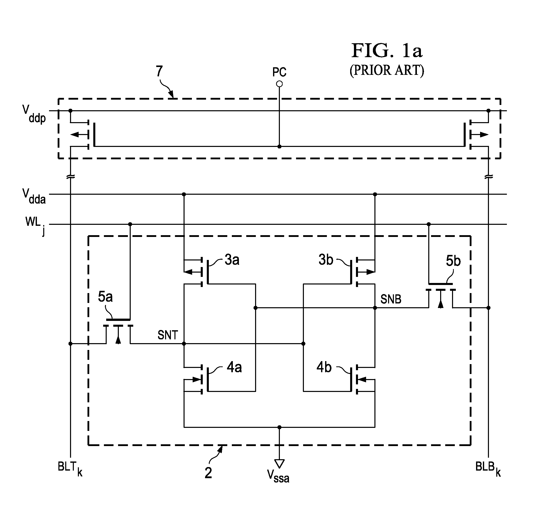
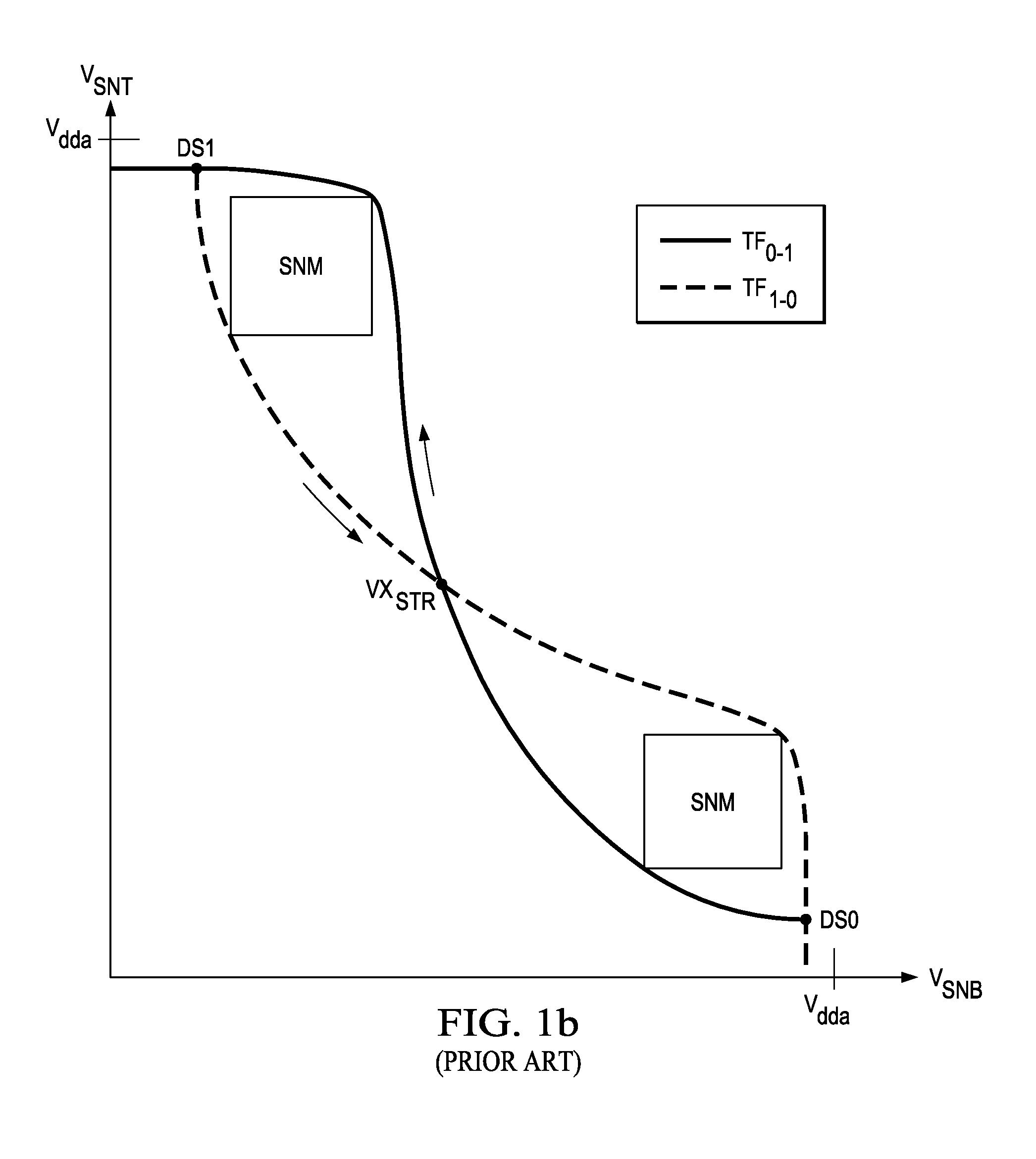
[0043]This invention will be described in connection with certain embodiments, namely as implemented into a method of testing static random access memories, because it is contemplated that this invention will be especially beneficial when used in such an application. However, it is also contemplated that embodiments of this invention will also be beneficial if applied to memories of other types, including read-only memories and electrically programmable read-only memories, among others. Furthermore, it is contemplated that embodiments of this invention may be used to test and screen circuit functions other than memories, including especially digital logic functions. Accordingly, it is to be understood that the following description is provided by way of example only, and is not intended to limit the true scope of this invention as claimed.

[0044]FIG. 2 illustrates an example of large-scale integrated circuit 10, in the form of a so-called “system-on-a-chip” (“SoC”), as now popular in...


PUM


Abstract

A method of screening complementary metal-oxide-semiconductor CMOS integrated circuits, such as integrated circuits including CMOS static random access memory (SRAM) cells, for n-channel transistors susceptible to transistor characteristic shifts over operating time. For the example of SRAM cells formed of cross-coupled CMOS inverters, static noise margin and writeability (Vtrip) screens are provided. Each of the n-channel transistors in the CMOS SRAM cells are formed within p-wells that are isolated from p-type semiconductor material in peripheral circuitry of the memory and other functions in the integrated circuit. Forward and reverse body node bias voltages are applied to the isolated p-wells of the SRAM cells under test to determine whether such operations as read disturb, or write cycles, disrupt the cells under such bias. Cells that are vulnerable to threshold voltage shift over time can thus be identified.

Description

CROSS-REFERENCE TO RELATED APPLICATIONS[0001]This application claims priority, under 35 U.S.C. §119(e), of Provisional Application No. 61 / 530,131, filed Sep. 1, 2011, which is incorporated herein by this reference.STATEMENT REGARDING FEDERALLY SPONSORED RESEARCH OR DEVELOPMENT[0002]Not applicable.BACKGROUND OF THE INVENTION[0003]This invention is in the field of solid-state memory. Embodiments of this invention are more specifically directed to the manufacture and testing of static random access memories (SRAMs).[0004]Many modern electronic devices and systems now include substantial computational capability for controlling and managing a wide range of functions and useful applications. Considering the large amount of digital data often involved in performing the complex functions of these modern devices, significant solid-state memory capacity is now commonly implemented in the electronic circuitry for these systems. Static random access memory (SRAM) has become the memory technolo...

Claims


Application Information

Patent Timeline
Patent Type & Authority Applications(United States)
IPC IPC(8): G11C29/00
CPCG11C11/41G11C29/50G11C29/06G11C29/50016G11C29/50004G11C2029/5002
Inventor SESHADRI, ANANDLOH, WAH KIT
Owner TEXAS INSTR INC
Why Eureka
Try Eureka