

Semiconductor device
- Summary
- Abstract
- Description
- Claims
- Application Information
AI Technical Summary
Benefits of technology
Problems solved by technology
Method used
Image

Examples
embodiment 1
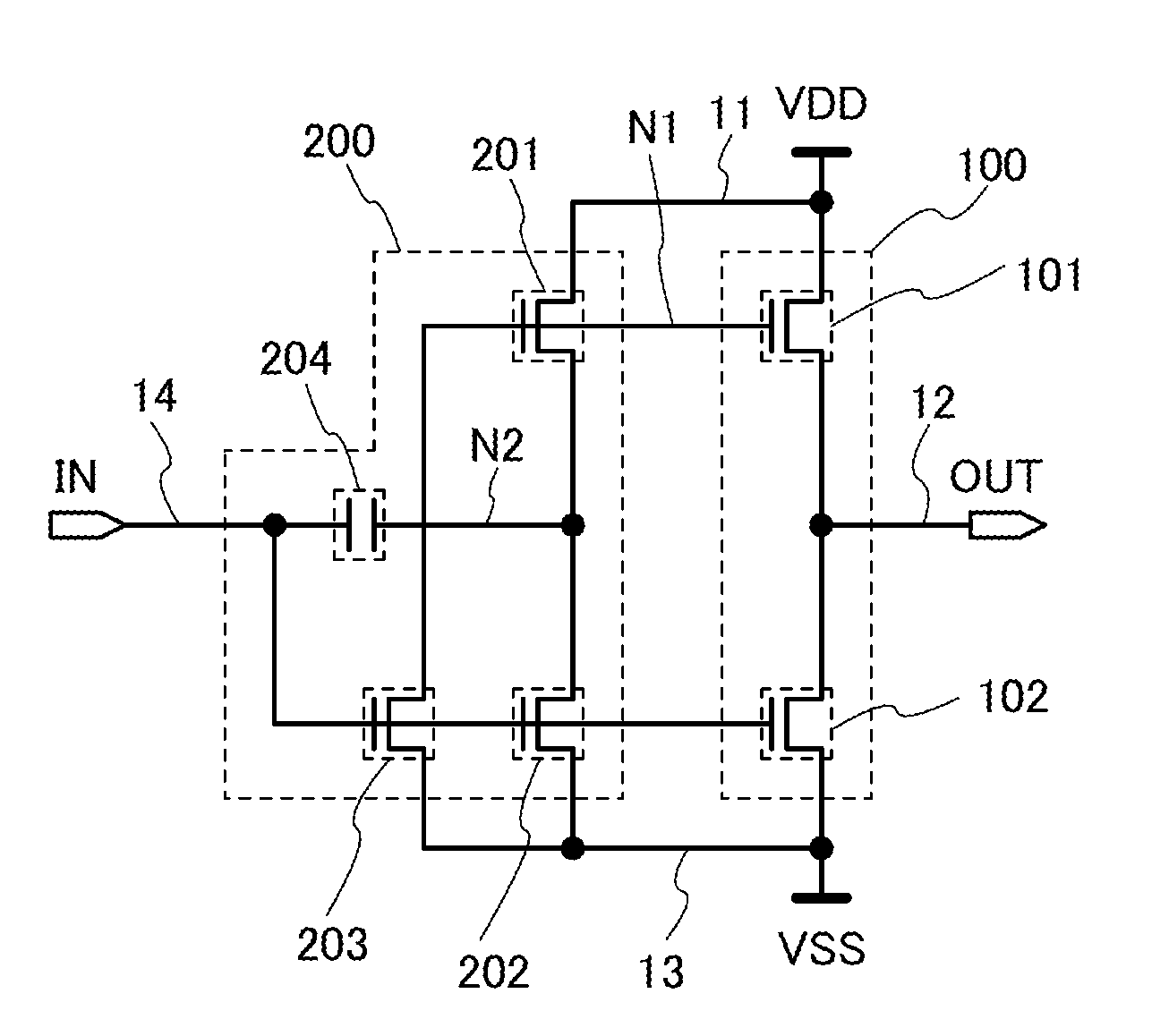
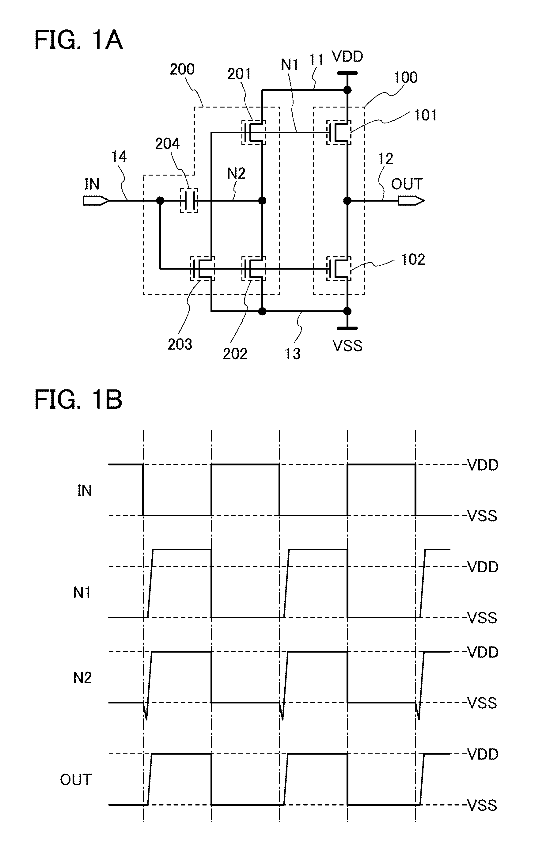
[0035]In Embodiment 1, an inverter circuit (also referred to as “semiconductor device” or “driver circuit”) according to one embodiment of the present invention will be described.
[0036]The configuration of an inverter circuit in this embodiment will be described with reference to FIG. 1A.
[0037]The inverter circuit illustrated in FIG. 1A includes a circuit 100 and a circuit 200. The circuit 100 is connected to a wiring 11, a wiring 12, a wiring 13, a wiring 14, and the circuit 200. The circuit 200 is connected to the wiring 11, the wiring 13, the wiring 14, and the circuit 100.
[0038]The circuit 100 includes a transistor 101 and a transistor 102. A first terminal (also referred to as “one of a source and a drain”) of the transistor 101 is connected to the wiring 11. A second terminal (also referred to as “the other of the source and the drain”) of the transistor 101 is connected to the wiring 12. A first terminal of the transistor 102 is connected to the wiring 13. A second terminal o...
embodiment 2
[0149]In Embodiment 2, a shift register circuit (also referred to as “semiconductor device” or “driver circuit”) according to one embodiment of the present invention will be described.
[0150]A shift register circuit in this embodiment includes a plurality of flip-flop circuits (also referred to as “semiconductor devices” or “driver circuits”). First, a flip-flop circuit will be described, and then a shift register circuit including the flip-flop circuit will be described.
[0151]A flip-flop circuit included in the shift register circuit of this embodiment will be described with reference to FIG. 7A.
[0152]The flip-flop circuit in FIG. 7A includes a transistor 401, a transistor 402, a transistor 403, a transistor 404, a transistor 405, and a circuit 500. A first terminal of the transistor 401 is connected to a wiring 21. A second terminal of the transistor 401 is connected to a wiring 22. A first terminal of the transistor 402 is connected to the wiring 13. A second terminal of the trans...
embodiment 3
[0235]Using an EL display device as an example, cross-sectional structures of a pixel and a driver circuit of a display device according to one embodiment of the present invention will be described with reference to FIG. 12. FIG. 12 exemplifies cross-sectional structures of a pixel 840 and a driver circuit 841.
[0236]The pixel 840 includes a light-emitting element 832 and a transistor 831 having a function of supplying current to the light-emitting element 832. In addition to the light-emitting element 832 and the transistor 831, the pixel 840 may also include a variety of semiconductor elements such as a transistor that controls input of an image signal to the pixel 840 and a capacitor that holds the potential of an image signal.
[0237]The driver circuit 841 includes a transistor 830 and a capacitor 833 for holding the gate voltage of the transistor 830. The driver circuit 841 corresponds to the inverter circuit in Embodiment 1 or the flip-flop circuit or the shift register circuit i...
PUM
 Abstract
Description
Claims
Application Information