Homogeneous multiple band gap devices

a multi-band gap, heterogeneous technology, applied in the direction of semiconductor devices, electrical devices, nanotechnology, etc., can solve the problems of 69 percent of solar energy not being cultivated, the semiconductor cannot absorb photons with energy, and the maximum efficiency that a photoelectric device can achieve, etc., to achieve the effect of improving efficiency and being easy to fabrica

Inactive Publication Date: 2013-04-25
UNIV OF UTAH RES FOUND
View PDF3 Cites 27 Cited by
  • Summary
  • Abstract
  • Description
  • Claims
  • Application Information

AI Technical Summary

Benefits of technology

[0012]The present disclosure provides improved devices that are easier to fabricate and / or have improved efficiency or other improved characteristics.

Problems solved by technology

Of the two classes, intrinsic factors set a limit on the maximum efficiency that a photoelectric device can achieve.
The first loss results from the failure of a semiconductor to absorb photons with energy less than the energy band gap of the semiconductor.
That is, 69 percent of solar energy is not cultivated due to the intrinsic losses.
Such requirements impose technical challenges in the fabrication of semiconducting materials and multijunction devices.
It is difficult to construct three different semiconducting materials having desired band gaps, and at the same time, meeting other design goals such as a matched lattice constant.
This leads to a non-ideal combination of band gaps, and consequently lower device efficiency.
Although modification of the composition of semiconducting materials may improve device efficiency, maximum efficiencies have not yet been achieved to date because of practical obstacles in building such devices.
Such obstacles include facilitating epitaxial growth of desired compositions due to miscibility gap of multiple layers on top of each other while satisfying interlayer lattice matching constraints and the need to balance the amount of current generated in each junction in the multijunction stack.
That is, composition tuning, lattice constant matching, and current balancing complicate the multijunction fabrication process and increase the cost of production of such devices.

Method used


Image

  • Homogeneous multiple band gap devices
  • Homogeneous multiple band gap devices
  • Homogeneous multiple band gap devices

Examples


Embodiment Construction

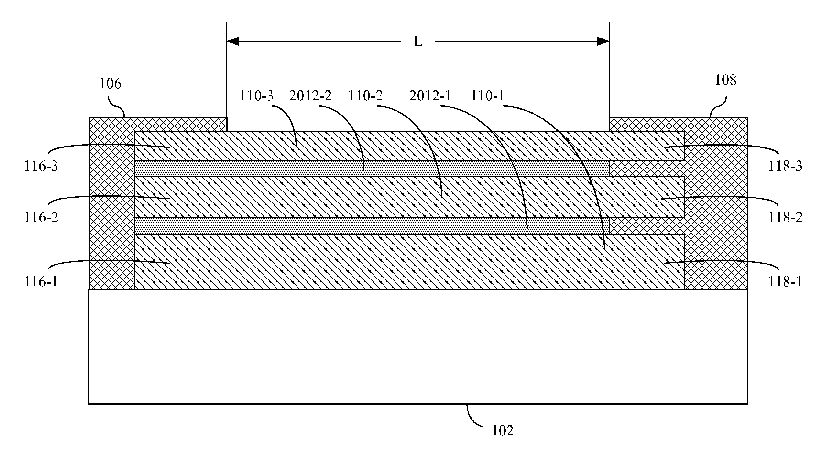
[0098]Disclosed herein are multiple band gap devices comprising a plurality of semiconducting nanoribbons disposed on a substrate or comprising a plurality of stacks disposed on a substrate with each stack having a plurality of semiconducting nanoribbons. Each nanoribbon in the plurality of semiconducting nanoribbons is characterized by a band gap, and is in electrical communication with two conductive leads.

[0099]Also disclosed herein are multiple band gap devices comprising one or more semiconducting nanohole superlattices comprising one or more stacks disposed on a substrate with each stack having one or more semiconducting nanohole superlattices. Each nanohole superlattice is characterized by a band gap range, and is in electrical communication with two conductive leads.

[0100]The instant multiple band gap devices can be used for various applications, for example, as photovoltaic solar cells for converting light into power, as photodetectors for converting an incident light into ...


PUM


Abstract

An electrical device comprising (A) a substrate having a surface and (B) a nanohole superlattice superimposed on a portion of the surface is provided. The nanohole superlattice comprises a plurality of sheets having an array of holes defined therein. The array of holes is characterized by a band gap or band gap range. The plurality of sheets forms a first edge and a second edge. A first lead comprising a first electrically conductive material forms a first junction with the first edge. A second lead comprising a second electrically conductive material forms a second junction with the second edge. The first junction is a Schottky barrier with respect to a carrier. In some instances a metal protective coating covers all or a portion of a surface of the first lead. In some instances, the first lead comprises titanium, the second lead comprises palladium, and the metal protective coating comprises gold.

Description

1. CROSS REFERENCE TO RELATED APPLICATIONS[0001]This application claims priority to U.S. Patent Application No. 61 / 615,130 entitled “Homogeneous Band Gap Devices Having A Lead With a Metal Protective Coating,” filed Mar. 23, 2012, which is hereby incorporated herein by reference. This application also claims priority to U.S. Patent Application No. 61 / 615,137 entitled “Homogeneous Multiple Band Gap Devices,” filed Mar. 23, 2012, which is hereby incorporated herein by reference. This application also claims priority to U.S. Patent Application No. 61 / 549,814 entitled “Graphene Nanohole Superlattice-based Photovoltaic Cells,” filed Oct. 21, 2011, which is hereby incorporated herein by reference.2. FIELD OF THE INVENTION[0002]This invention relates to band gap devices for converting photon energy into a voltage or current, or for converting a current into photon energy, over a broad wavelength spectrum, and more particularly to multiple band gap devices comprising nanohole superlattices....

Claims


Application Information

Patent Timeline
Patent Type & Authority Applications(United States)
IPC IPC(8): H01L31/0352H01L33/06
CPCH01L31/035236H01L31/07H01L33/06H01L33/08H01L33/40H01L31/035209H01L31/1013Y02E10/50H01L33/0041H01L31/032B82Y20/00Y02E10/52Y02E10/547
Inventor LIU, FENGZHANG, YESUN, RUJIE
Owner UNIV OF UTAH RES FOUND
Why Eureka
Try Eureka