Silicon submount for light emitting diode and method of forming the same

Inactive Publication Date: 2013-05-02
EPISIL TECH
View PDF2 Cites 25 Cited by
  • Summary
  • Abstract
  • Description
  • Claims
  • Application Information

AI Technical Summary

Benefits of technology

[0008]The invention is directed to a silicon submount of a light emitting diode (LED) that is characterized by both i

Problems solved by technology

The submount is often made of a resin material (e.g., epoxy resin), and the resin material exposed to ultraviolet radiation over a long period is very much likely to encount

Method used


Image

  • Silicon submount for light emitting diode and method of forming the same
  • Silicon submount for light emitting diode and method of forming the same
  • Silicon submount for light emitting diode and method of forming the same

Examples


Example

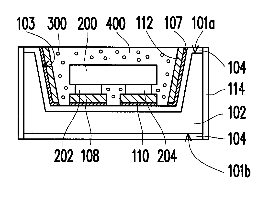
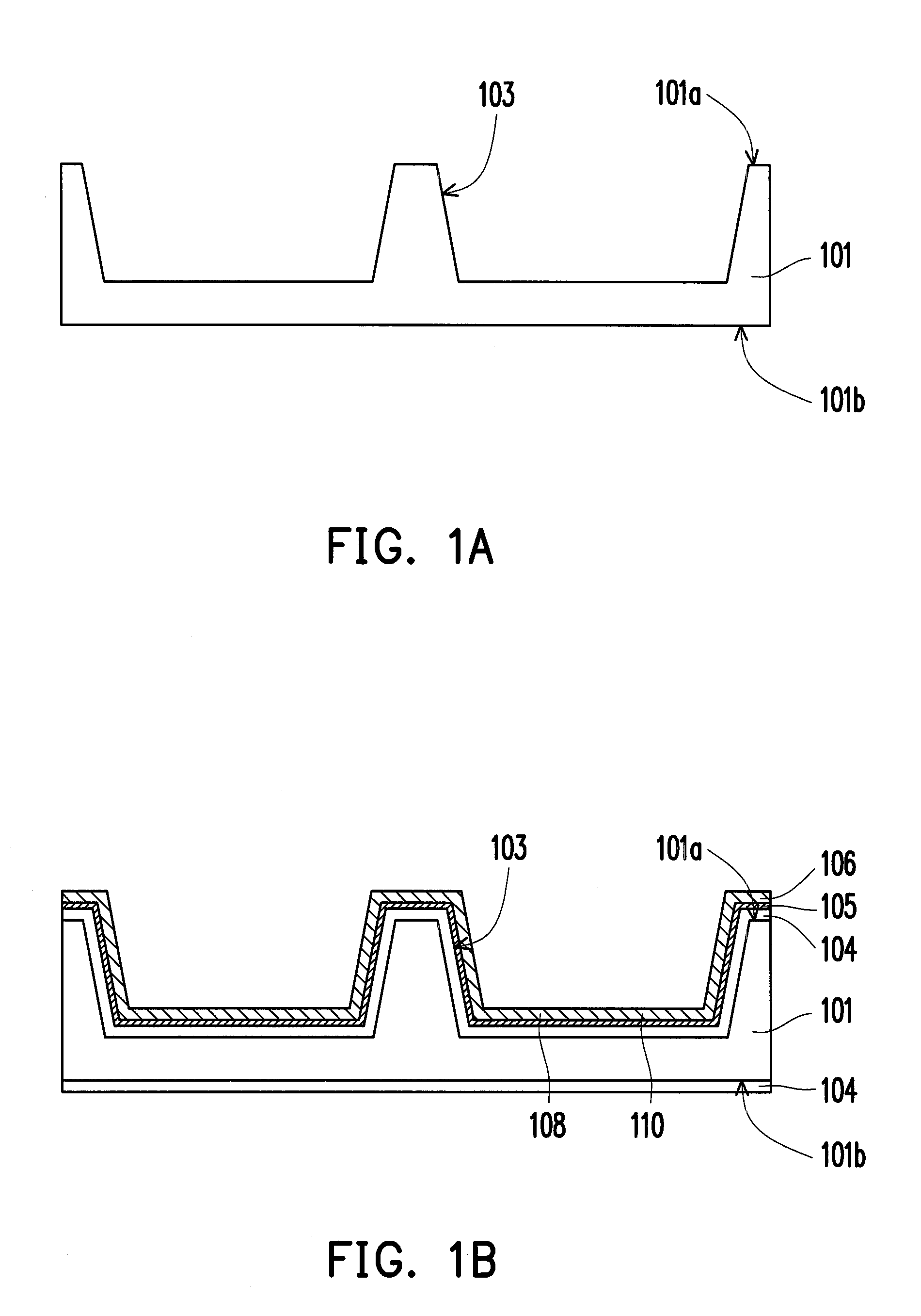
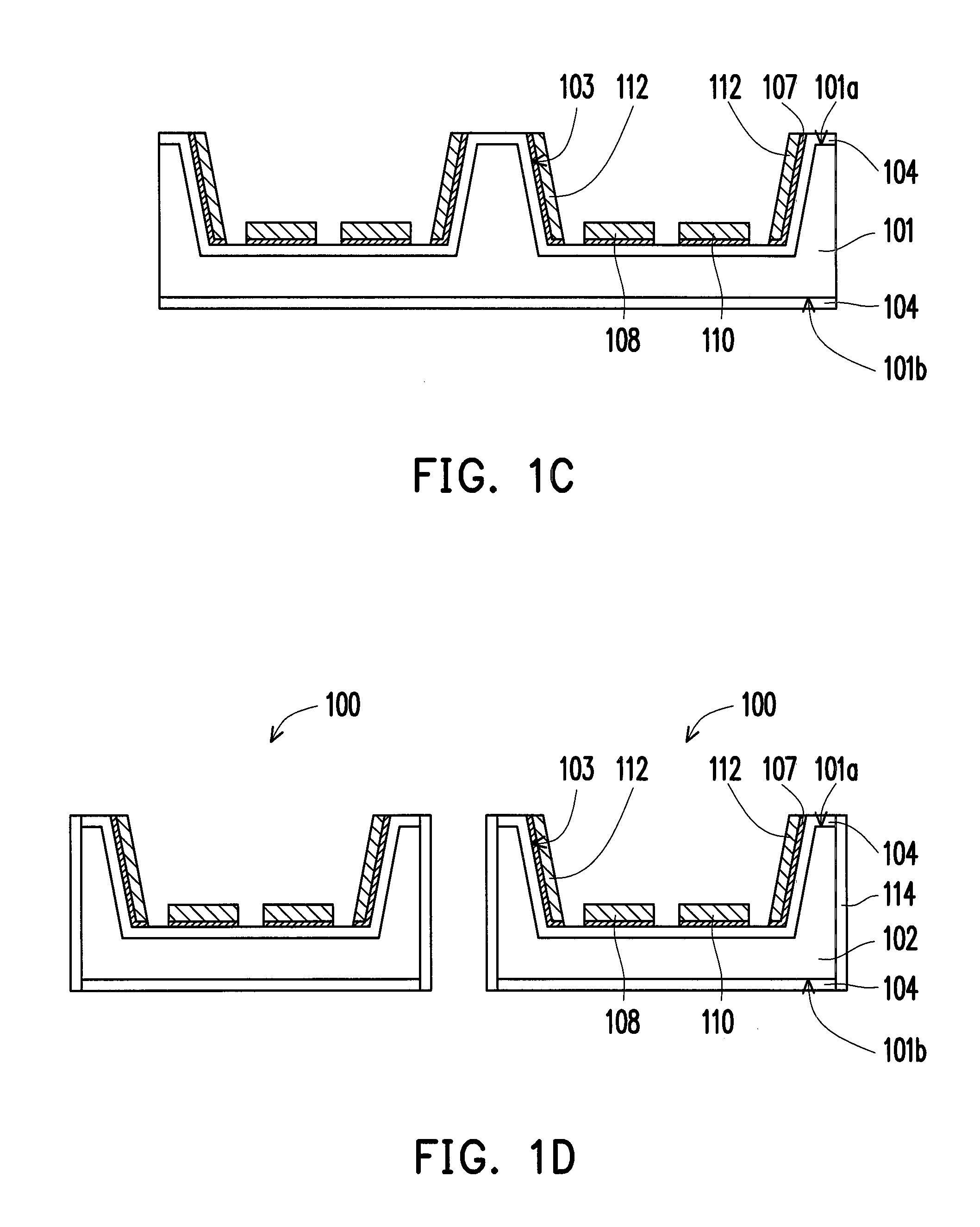
[0033]FIG. 1A to FIG. 1D are schematic cross-sectional views illustrating a method of forming a silicon submount for an LED according to a first embodiment of the invention.

[0034]With reference to FIG. 1A, a silicon substrate 101 is provided. The silicon substrate 101 has an upper surface 101a and a lower surface 101b. A plurality of recesses 103 are formed at the upper surface 101a of the silicon substrate 101. Each recess 103 has an inclined sidewall, for instance. Steps of forming the recess 103 are described below. First, an oxide pad layer, a silicon nitride layer, and a patterned photoresist layer (not shown) are sequentially formed on the upper surface 101a of the silicon substrate 101. An etching process is performed with use of the patterned photoresist layer as a mask, so as to form a patterned oxide pad layer and a patterned silicon nitride layer. The patterned photoresist layer is removed. A wet etching process is performed with use of the patterned oxide pad layer and t...


PUM


Abstract

A silicon submount for a light emitting diode (LED) including a silicon base, a first insulating layer, a first electrode, a second electrode, and a reflective layer is provided. The silicon base has an upper surface and a lower surface, and a recess is disposed at the upper surface. The first insulating layer covers the upper surface and the lower surface of the silicon base. The first electrode and the second electrode are disposed on the first insulating layer on a bottom of the recess. The reflective layer is disposed on the first insulating layer on a sidewall of the recess. The first electrode, the second electrode, and the reflective layer are separated from one another and formed by the same material.

Description

CROSS-REFERENCE TO RELATED APPLICATION[0001]This application claims the priority benefit of Taiwan application serial no. 100138925, filed on Oct. 26, 2011. The entirety of the above-mentioned patent application is hereby incorporated by reference herein and made a part of this specification.BACKGROUND OF THE INVENTION[0002]1. Field of the Invention[0003]The invention relates to a semiconductor component and a method of forming the same. More particularly, the invention relates to a silicon submount for a light emitting diode (LED) and a method of forming the same.[0004]2. Description of Related Art[0005]The mechanism of a light emitting diode (LED) relates to light emission resulting from the energy that is released when electrons and holes in a semiconductor material are combined. Due to numerous advantages of the LED including compact volume, durability, low driving voltages, low electricity consumption, fast response speed, great resistance to vibration, and favorable monochroma...

Claims


Application Information

Patent Timeline
IPC IPC(8): H01L23/532H01L21/768
CPCH01L33/60H01L33/62H01L2224/16H01L2933/0033H01L33/641
Inventor HUNG, CHIH-LUNG
Owner EPISIL TECH
Why Eureka
Try Eureka