Functionalized nanostructures for detecting nitro-containing compounds
a technology of nitro-containing compounds and functionalized nanostructures, which is applied in the field of detection of chemicals, can solve the problems of posing a huge challenge, the low volatility of many target analytes in the detection method of traces of explosives, and the threat of direct security
- Summary
- Abstract
- Description
- Claims
- Application Information
AI Technical Summary
Benefits of technology
Problems solved by technology
Method used
Image
Examples
example 1
Nanowire FET Fabrication
[0307]Silicon nanowires (SiNWs) were synthesized by chemical vapor deposition (CVD) with the use of 20 nm gold nanoparticles as catalysts and silane as reactant. Diborane was used during the growth to provide boron as a p-type dopant with a B:Si ratio of 1:4000. The FETs were fabricated by photolithography. Briefly, passivated source and drain electrodes were deposited with the use of a multilayer photoresist structure consisting of 300 nm LOR3A (Microchem) and 500 nm 1805 (Shipley). After exposure and development of the electrode pattern, the contacts were metallized by e-beam and thermal evaporation of Ti / Pd (5 / 60 nm) respectively and were then passivated from the electrolyte with an insulating layer of Si3N4 (50 nm-thick) deposited by plasma-enhanced chemical vapor deposition (PECVD). The separation between the source and drain electrodes for each FET was 2 μm. Last, the chip was coated with a 100 μm SU-8 3050 photoresist (Microchem Inc.) and a channel was...
example 2
Fluid-Delivery System
[0308]The fluid-delivery device was fabricated from flexible polydimethylsiloxane (PDMS) elastomer mixed in a 10:1 ratio of base to curing agent. The PDMS was cured overnight in an oven at 60° C. and then cut into rectangular pieces. The dimensions of the PDMS were 10×10×5 mm (length×width×height). The lithographically-defined SU-8 channel sealed by the PDMS elastomer created a fluid delivery system.
example 3
Surface Modification of Nanowire Device
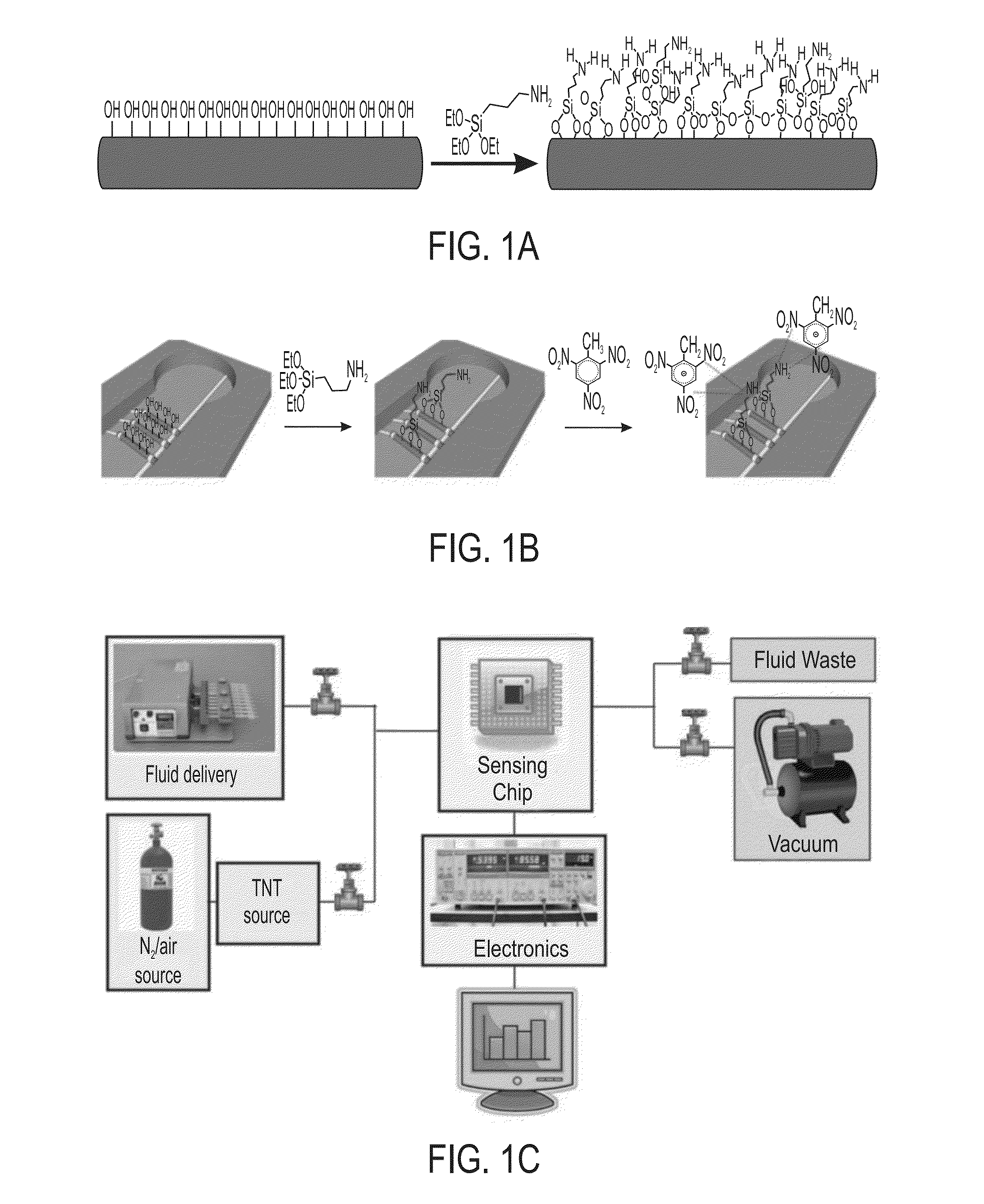
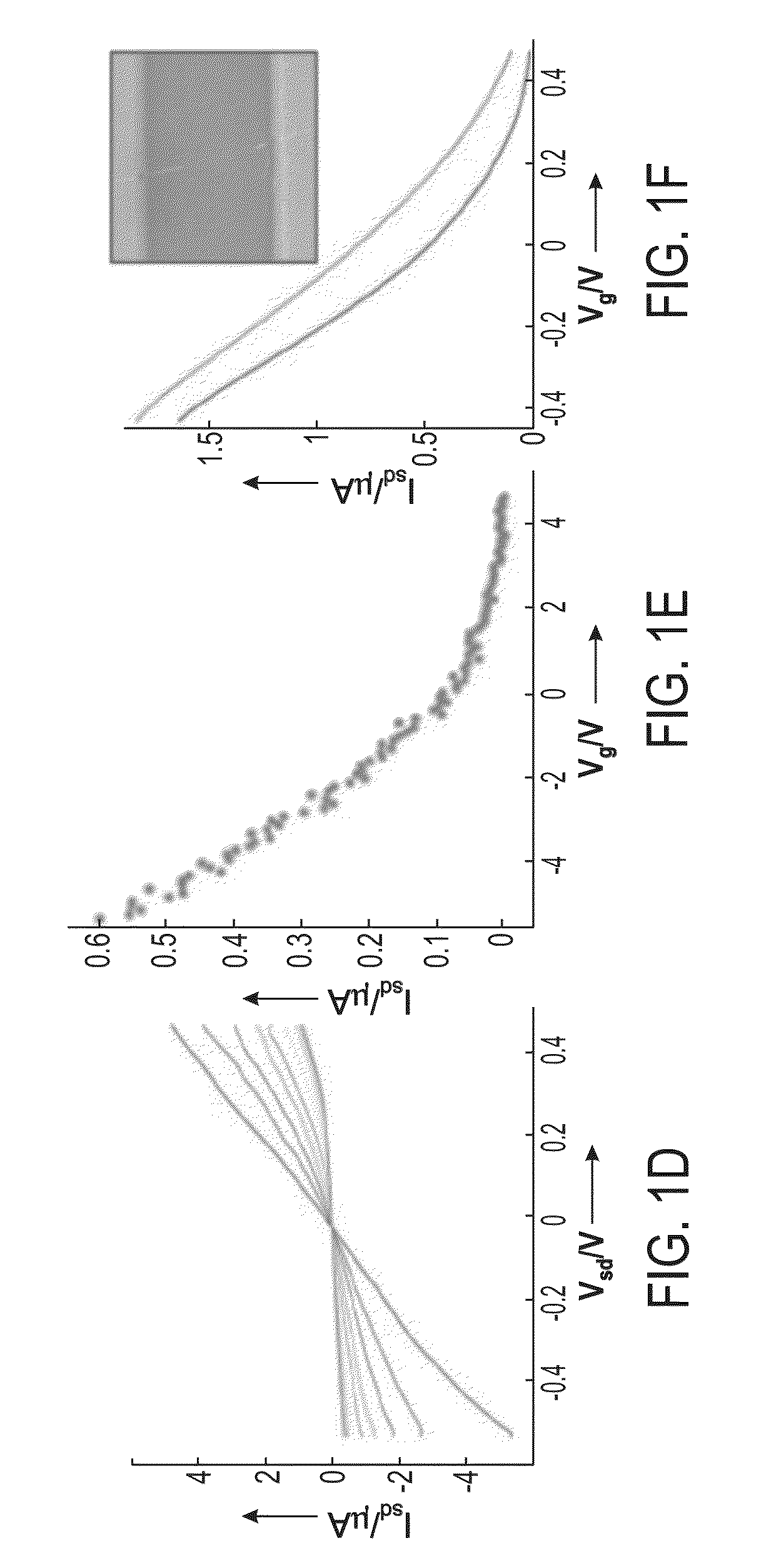
[0309]The chemical modification of the sensing elements and the electrical-transport characteristics of the devices obtained were studied. Amino-functionalized layers were prepared by self-assembling 3-aminopropyltriethoxysilane (APTES) on silicon-nanowire devices in aqueous solutions for varied deposition times.
[0310]The sensor device was cleaned with oxygen plasma, so as to obtain clean and oxidized nanowire-device surfaces for the effective chemical modification with 3-aminopropyltriethoxysilane to provide amino groups at the nanowire surface. The chip was first treated with 1% (v / v) 3-aminopropylethoxysilane (APTES) (Aldrich) in 95% ethanol, and was allowed to stand for 20 minutes before filtering through a 0.2 μm-cutoff syringe filter. The plasma-cleaned sensor chip was immersed in the silane / ethanol solution for 30 minutes and then the chip was rinsed with ethanol, dried in a stream of nitrogen gas and baked at 150° C. for 5 minutes.
[0311...
PUM
 Abstract
Description
Claims
Application Information


