
Methods for depositing nickel films and for making nickel silicide and nickel germanide

a technology of metal silicide and germanide, which is applied in the manufacturing of semiconductor/solid-state devices, basic electric elements, electrical equipment, etc., can solve the problems of low resistance silicide on the top of the gate, source, drain and any other exposed silicon surface, and process may not be effective in all contexts. , the coverage of ni over the three-dimensional structure is poor

Active Publication Date: 2013-05-09
ASM INTERNATIONAL
View PDF4 Cites 403 Cited by
  • Summary
  • Abstract
  • Description
  • Claims
  • Application Information

AI Technical Summary

Benefits of technology

The patent text describes methods for depositing nickel thin films using vapor deposition processes. The methods involve alternately and sequentially contacting a substrate with a vapor phase nickel precursor and a second reactant, such as a reducing agent or an organic reducing agent, to form a layer of nickel precursor on the substrate surface. Annealing is then carried out to form a nickel thin film. The methods can be used to deposit nickel onto silicon or germanium substrates, and can also be used to form metal silicide or germanide layers. The technical effects of the methods include the ability to deposit thin films of nickel with controlled thickness and composition, and the ability to form doped metal silicides or germanides with desired dopant concentrations.

Problems solved by technology

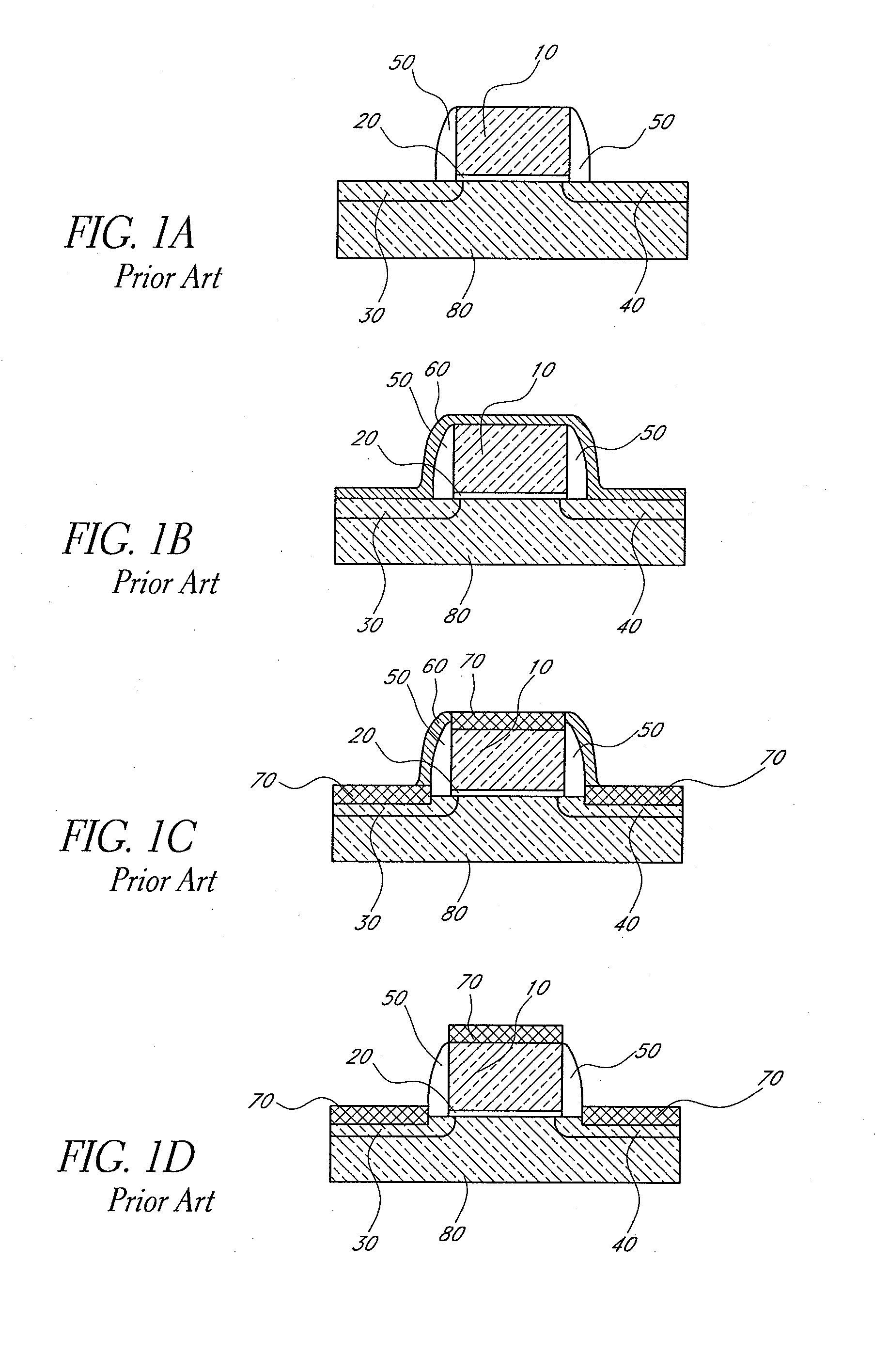
This results in a low-resistivity silicide on top of the gate, source, drain and any other exposed silicon surfaces.
In practice, however, this process may not be effective in all contexts.
The result is that the step coverage of the Ni over the three-dimensional structure is poor due, at least in part, to the limitations in the PVD processes used for depositing the Ni.
Such variation is undesirable because it can introduce non-uniformities in the electrical performance of electrical devices formed using the NiSix films.
Depositing metal by more conformal processes like chemical vapor deposition (CVD) or atomic layer deposition (ALD) has not been straightforward.

Method used


Image

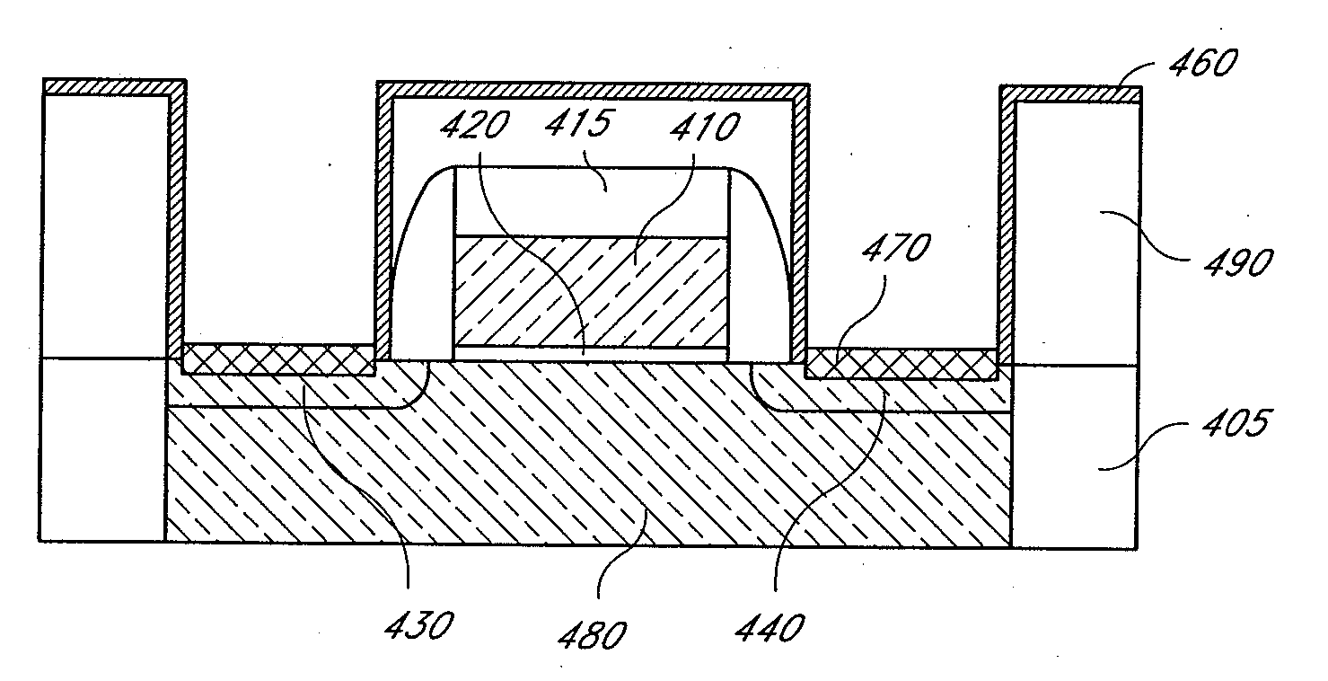
  • Methods for depositing nickel films and for making nickel silicide and nickel germanide
  • Methods for depositing nickel films and for making nickel silicide and nickel germanide
  • Methods for depositing nickel films and for making nickel silicide and nickel germanide

Examples


example 1

[0281]Experiments were conducted using ALD of Sb for the interface layer, followed by ALD of metal oxide over the interface layer, followed by an anneal in a reducing environment that accomplished both reduction of the metal oxide and silicidation of the underlying silicon through the interface layer.

[0282]Initially, 5 cm×5 cm silicon substrates were dipped in 1% aqueous HF solution for native oxide cleaning. Sb was then deposited by ALD at 100° C. using a F-120 research scale reactor. SbCl3 and (EtsSi)3Sb were alternately pulsed with intervening purging for 100 cycles. Reactant pulse / purge lengths were ⅓ s for SbCl3 and ⅔ s for (EtsSi)3Sb. Subsequently, NiO was deposited by ALD in a Pulsar 2000 ALCVD prototype reactor at 160° C. by alternately pulsing bis(4-N-ethylamino-3-penten-2-N-ethyliminato)nickel (II) and O3. Pulse durations of 1 s and purge durations of 4 s were used for both reactants, and 2000 cycles were performed. Post-deposition annealing was conducted for 1 minute at ...

example 2

[0284]Experiments were conducted using epitaxial Ge for the interface layer, followed by ALD of metal oxide over the interface layer, followed by an anneal in a reducing environment that accomplished both reduction of the metal oxide, germanidation of the interface layer and silicidation of the underlying silicon through the interface layer.

[0285]Continuous Ge films with thickness from about 7 to about 15 nm were deposited by CVD on silicon at 350° C. by using deposition times from about 150 seconds to about 210 seconds. Surface roughnesses of the Ge films were about 0.6 nm. NiO was deposited by ALD in a Pulsar 2000 ALCVD prototype reactor at 160° C. by alternately pulsing bis(4-N-ethylamino-3-penten-2-N-ethyliminato)nickel (II) and O3. Pulse durations of 1 s and purge durations of 4 s were used for both reactants, and 2000 cycles were performed. Post-deposition annealing was conducted for 10 minutes at 450° C. in 1 atmosphere partial pressure of forming gas (5% / 95% H2 / N2).

[0286]Cry...

example 3

[0287]Experiments were conducted using epitaxial Ge films on Si of 1 μm in thickness followed by ALD of metal oxide over the Ge film, followed by an anneal in a reducing environment that accomplished both reduction of the metal oxide and germanidation of the underlying germanium.

[0288]NiO was deposited by ALD in a Pulsar 2000 ALCVD prototype reactor at 160° C. by alternately pulsing bis(4-N-ethylamino-3-penten-2-N-ethyliminato)nickel (II) and O3. Pulse durations of 1 s and purge durations of 4 s were used for both reactants, and 2000 cycles were performed. In-situ) (RD was done using an HTK 1200N oven commercially available from Anton Paar GmbH of Österich, Austria, and the PANalytical X'PERT PRO MPD diffractometer in forming gas (5 / 95% H2 / N2) up to 600° C.

[0289]FIG. 9 illustrates the results of the x-ray diffraction (XRD) analyses, showing composite images for annealing the nickel oxide over germanium at different temperatures. The NiO reflections disappear at 250° C., and NiGe beg...


PUM


Abstract

In one aspect, methods of silicidation and germanidation are provided. In some embodiments, methods for forming metal silicide can include forming a non-oxide interface, such as germanium or solid antimony, over exposed silicon regions of a substrate. Metal oxide is formed over the interface layer. Annealing and reducing causes metal from the metal oxide to react with the underlying silicon and form metal silicide. Additionally, metal germanide can be formed by reduction of metal oxide over germanium, whether or not any underlying silicon is also silicided. In other embodiments, nickel is deposited directly and an interface layer is not used. In another aspect, methods of depositing nickel thin films by vapor phase deposition processes are provided. In some embodiments, nickel thin films are deposited by ALD. Nickel thin films can be used directly in silicidation and germanidation processes.

Description

CROSS-REFERENCE TO RELATED APPLICATIONS[0001]This application claims priority to U.S. Provisional application No. 61 / 526,607, filed Aug. 23, 2011, the disclosure of which is incorporated herein.[0002]This application is also related to U.S. patent application Ser. No. 12 / 339,672, filed Dec. 19, 2008, and International Application No. PCT / US10 / 53982, filed Oct. 25, 2010. The entire contents of all of the above applications are hereby incorporated by reference and should be considered a part of this specification.BACKGROUND OF THE INVENTION[0003]1. Field of the Invention[0004]The invention relates generally to the field of semiconductor device manufacturing and, more particularly, to methods for depositing nickel and forming metal silicide and germanide.[0005]2. Description of the Related Art[0006]In forming advanced semiconductor devices, part of the silicon that is present in gate, source and drain structures can be converted into low-resistivity metal silicides. This is done to rea...

Claims


Application Information

Patent Timeline
IPC IPC(8): H01L21/768
CPCH01L21/76886H01L29/78H01L29/665H01L21/28052H01L21/76843H01L21/76855H01L21/28518H01L21/28568H01L21/321H01L21/32133H01L21/3215H01L29/456
Inventor PORE, VILJAMI J.HAUKKA, SUVI P.BLOMBERG, TOM E.TOIS, EVA E.
Owner ASM INTERNATIONAL
Learn More