Semiconductor surface light-emitting element and method of manufacturing thereof

a technology of semiconductor layer and light-emitting element, which is applied in the direction of optical elements, semiconductor lasers, instruments, etc., can solve the problems of difficult to produce a large-area 2dpc, wafers cannot be well bonded to each other, and are not suitable for large-area implementation, so as to improve the crystallinity of the semiconductor layer forming it, improve the emission output and lifetime, and improve the effect of crystallinity

Active Publication Date: 2013-05-16
HAMAMATSU PHOTONICS KK +1
View PDF4 Cites 15 Cited by
  • Summary
  • Abstract
  • Description
  • Claims
  • Application Information

AI Technical Summary

Benefits of technology

[0021]With the semiconductor surface light-emitting element and manufacturing method thereof according to one aspect of the present invention, the crystallinity of the semiconductor layer forming it is improved and it is thus feasible to improve the properties such as emission output and lifetime.

Problems solved by technology

(1) It is difficult to produce a large-area 2DPC.
Specifically, for example, when wafers to be bonded are warped, when there is dust between wafers, or when wafer surfaces are significantly uneven, these wafers cannot be well bonded to each other.
(2) The 2DPC layer includes cavities and the coupling coefficient K is large, which is not suitable for implementation of large area.
(3) There are defects formed at the interface between the bonded wafers, which leads 10 to drawbacks in lifetime and reliability.

Method used


Image

  • Semiconductor surface light-emitting element and method of manufacturing thereof
  • Semiconductor surface light-emitting element and method of manufacturing thereof
  • Semiconductor surface light-emitting element and method of manufacturing thereof

Examples


Embodiment Construction

[0052]A semiconductor surface light-emitting element and manufacturing method thereof according to an embodiment will be described below. The same elements will be denoted by the same reference signs, without redundant description.

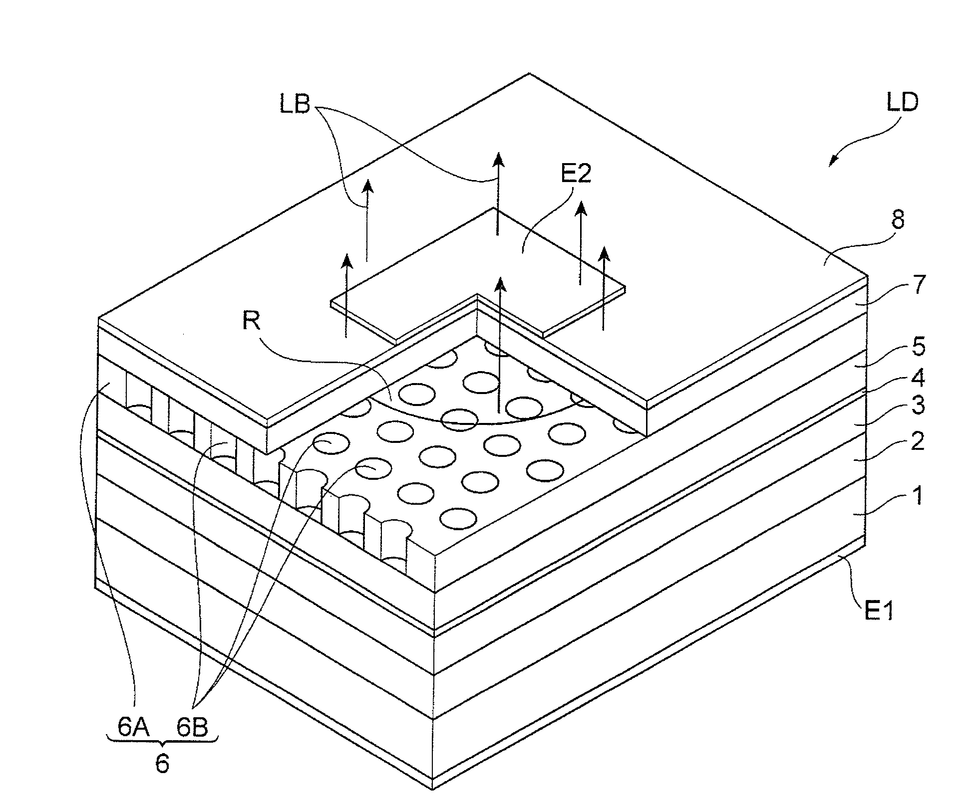
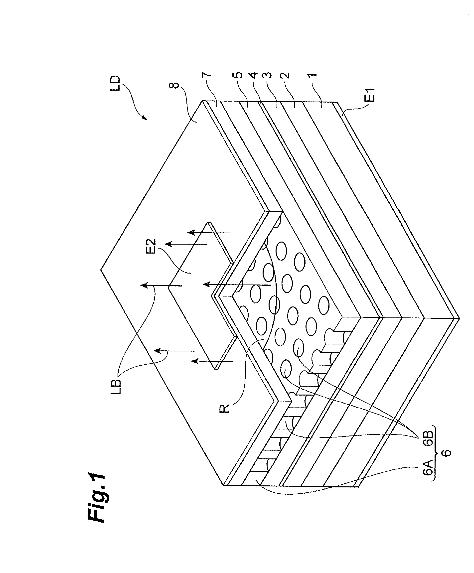
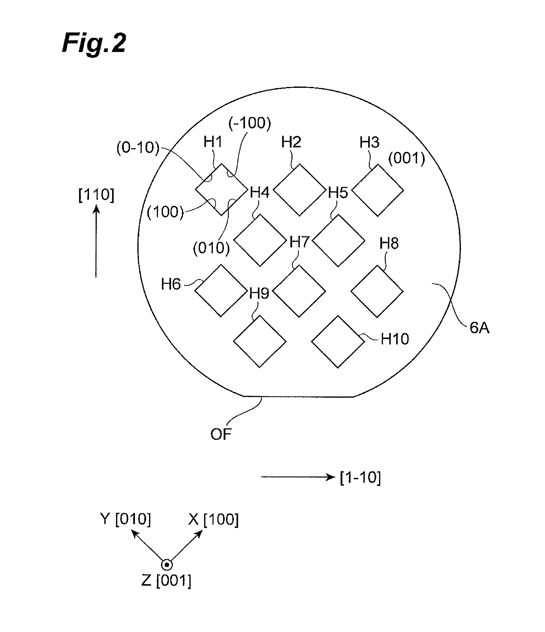
[0053]FIG. 1 is a perspective view of the semiconductor surface light-emitting element a part of which is broken.

[0054]The semiconductor surface light-emitting element is provided with a lower cladding layer 2, a lower light guiding layer 3, an active layer 4, an upper light guiding layer 5, a photonic crystal layer 6, an upper cladding layer 7, and a contact layer 8 which are successively formed on a semiconductor substrate 1. An electrode E1 is provided over the entire surface on the back side of the semiconductor substrate 1, and an electrode E2 in a central region of the contact layer 8.

[0055]Materials / thicknesses of these compound semiconductor layers are as described below. The layers without conductivity type are intrinsic semiconductors an impurity...


PUM


Abstract

A semiconductor surface light-emitting element of this invention is provided with a photonic crystal layer 6 obtained by periodically forming a plurality of holes H in a basic layer 6A comprised of a first compound semiconductor of the zinc blende structure and growing embedded regions 6B comprised of a second compound semiconductor of the zinc blende structure, in the holes H, and an active layer 4 to supply light to the photonic crystal layer 6, in which a principal surface of the basic layer 6A is a (001) plane and in which side faces of each hole H have at least three different {100} facets.

Description

TECHNICAL FIELD[0001]An aspect of the present invention relates to a semiconductor surface light-emitting element and a manufacturing method thereof.BACKGROUND ART[0002]A photonic crystal is a nanostructure in which the refractive index varies on a periodic basis, and can control wavelengths of light passing through it. A photonic crystal surface light-emitting laser (referred to hereinafter as PCSEL) using a two-dimensional photonic crystal (referred to hereinafter as 2DPC) is proposed as a next-generation semiconductor surface light-emitting element. PCSEL is characterized in that the optical properties thereof are determined by the size and shape of microstructure, independent of materials, and has new properties hard to be achieved by the conventional semiconductor light-emitting elements alone, such as large area and single mode, two-dimensional polarization control, and control of emission angle, leading to a potential to develop a probability of a high-output semiconductor la...

Claims


Application Information

Patent Timeline
Patent Type & Authority Applications(United States)
IPC IPC(8): H01S5/30H01L33/00H01S5/185
CPCB82Y20/00G02B6/1225H01L2933/0083H01S5/105H01S5/3013H01S5/3202H01S5/3432H01S2304/04H01L33/005H01S5/18H01S5/11H01S5/185
Inventor HIROSE, KAZUYOSHIFURUTA, SHINICHIWATANABE, AKIYOSHISUGIYAMA, TAKAHIROSHIBATA, KOUSUKEKUROSAKA, YOSHITAKANODA, SUSUMU
Owner HAMAMATSU PHOTONICS KK
Why Eureka
Try Eureka