

Semiconductor device
a technology of semiconductors and devices, applied in the direction of semiconductor devices, electrical equipment, transistors, etc., to achieve the effect of reducing malfunctions
- Summary
- Abstract
- Description
- Claims
- Application Information
AI Technical Summary
Benefits of technology
Problems solved by technology
Method used
Image

Examples
embodiment 1
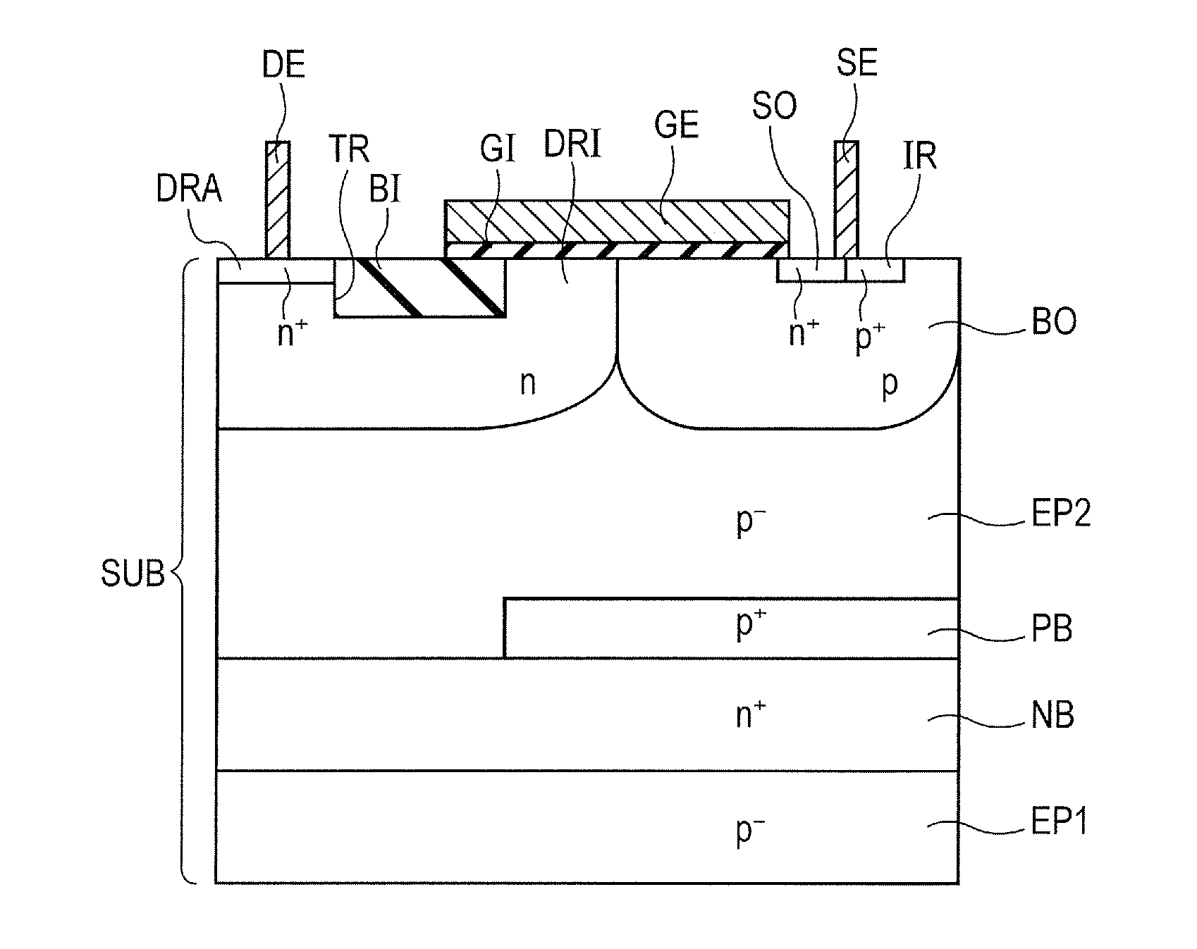
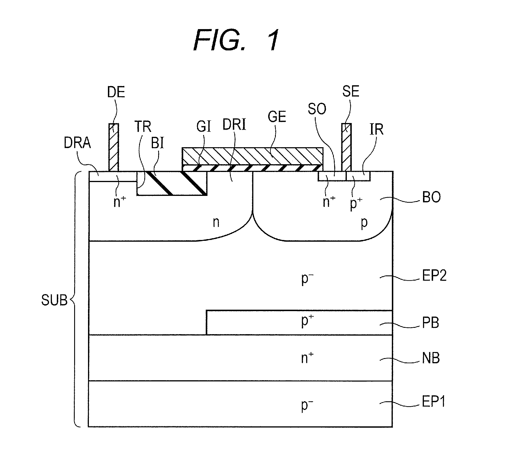
[0058]Firstly, the configuration of a semiconductor device according to the present embodiment is explained in reference to FIG. 1.
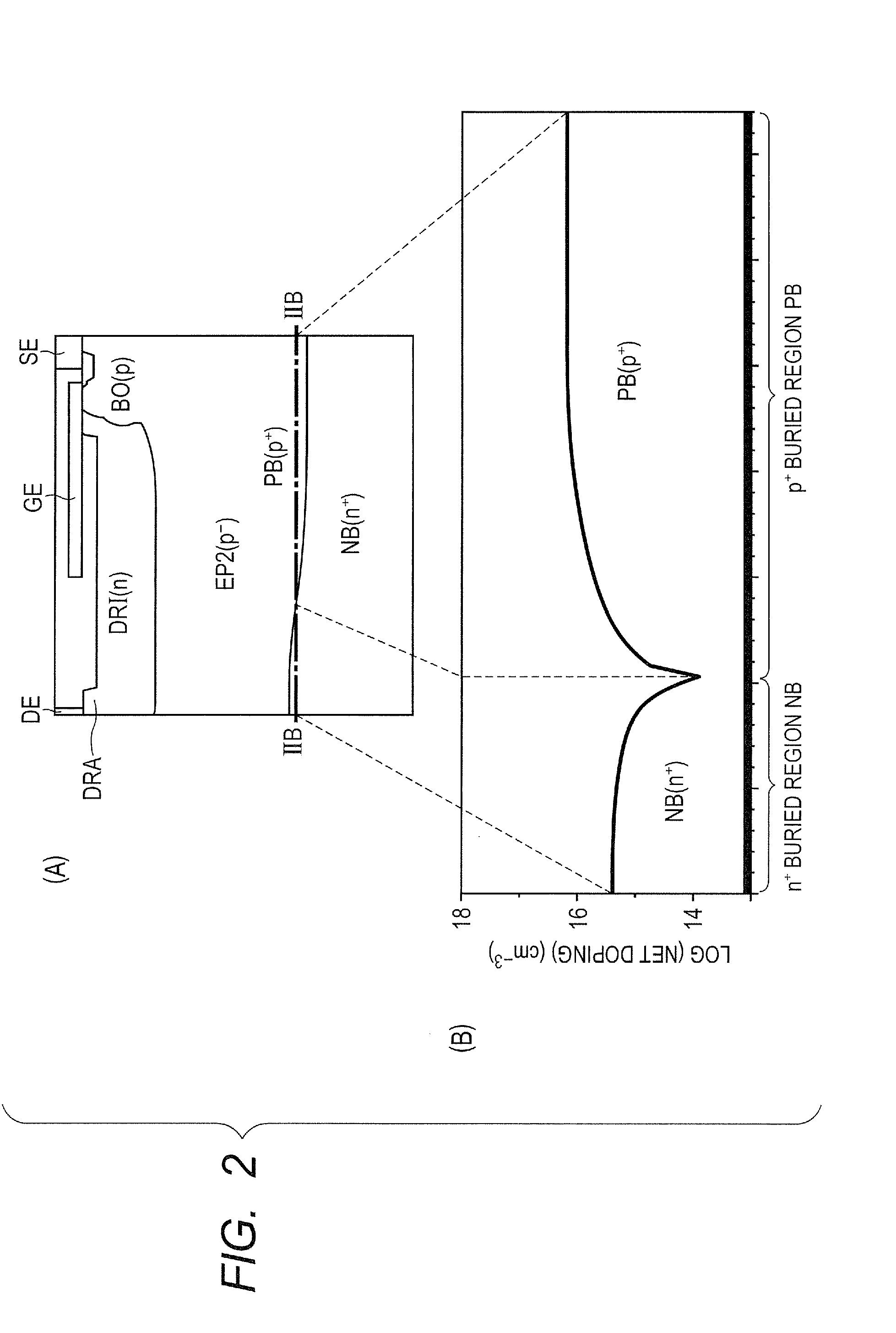
[0059]In reference to FIG. 1, a semiconductor device according to the present embodiment has an LDMOS transistor (lateral insulation gate type field effect transistor) for example. The semiconductor device mostly has a semiconductor substrate SUB, a p− epitaxial region (first region) EP1, an n+ buried region (fifth region) NB, a p+ buried region (sixth region) PB, a p− epitaxial region (second region) EP2, an n-type drift region (third region) DRI, a p-type body region (fourth region) BO, an n+ drain region (drain region) DRA, an n+ source region SO, a gate insulation film GI, a gate electrode layer GE, and an STI structure TR and BI.
[0060]The semiconductor substrate SUB includes silicon for example. The semiconductor substrate SUB has a main surface (a plane on the upper side in the figure). Thep− epitaxial region EP1 is formed in the semiconductor subs...
embodiment 2
[0125]Firstly, the configuration of a semiconductor device according to the present embodiment is explained in reference to FIGS. 30A and 30B.
[0126]In reference to FIG. 30A, a semiconductor device according to the first example of the present embodiment basically has a configuration similar to that of FIG. 1 according to Embodiment 1 but further has an n-type region (seventh region) NR.
[0127]An n-type region NR is formed in a semiconductor substrate SUB so as to reach an n+ buried region NB from the main surface of the semiconductor substrate SUB. The n-type region NR has an n-type diffusion region DNW extending from the main surface side so as to reach the n+ buried region NB and an n-type contact region NCR being formed over the main surface and having an n-type impurity concentration higher than that in the n-type diffusion region DNW. An electrode DE to which a drain potential is applied is formed over the main surface of the semiconductor substrate SUB so as to be electrically ...
embodiment 3
[0143]In an analog-digital consolidated technology, an LDMOS transistor like Embodiment 1 is sometimes formed over one chip through a process identical to the process of a CMOS (Complementary MOS), a bipolar transistor, a diode, a memory device, etc. When a transistor according to Embodiment 1 is laid out over such a chip, it is necessary to electrically isolate the transistor from other elements. In the present embodiment, a structure for electrical isolation is explained in reference to FIGS. 34 and 35.
[0144]In reference to FIGS. 34 and 35, in the present embodiment, an n-type diffusion region DNW (seventh region) is formed so as to surround the circumference of a region ARA where an array (lateral elements) in which the layout of LDMOS transistors shown in FIGS. 3A and 3B for example is repeated is allocated in a planar view. The n-type diffusion region DNW is formed in a semiconductor substrate SUB so as to reach an n+ buried region NB from the main surface of the semiconductor ...
PUM
 Abstract
Description
Claims
Application Information