Eureka AIR delivers breakthrough ideas for toughest innovation challenges, trusted by R&D personnel around the world.

Semiconductor device manufacturing method

Active Publication Date: 2013-05-30
INST OF MICROELECTRONICS CHINESE ACAD OF SCI
View PDF0 Cites 7 Cited by
  • Summary
  • Abstract
  • Description
  • Claims
  • Application Information

AI Technical Summary

Benefits of technology

The invention relates to a method for manufacturing semiconductor devices using a gate-last process. The method aims to obtain a smooth surface for the interlayer dielectric layer by using an etching process instead of a chemical mechanical polishing process. The technical effect of this method is to improve device performance and reliability.

Problems solved by technology

Polysilicon gates prevent further improvement of the performance of metal oxide semiconductor (MOS) devices when the size of the devices is continuously reduced, due to the excessive large resistance of the gates, polysilicon depletion effect and boron penetration effect in PMOS transistors.
Meanwhile, a serious interface defect is usually formed when integrating a polysilicon gate with a high K gate dielectric, which results in a pinning phenomenon of the device threshold and reduction in carrier mobility in channel.
Thus in the gate-first process, the materials of the metal gate are limited, which accordingly limits the increase of the threshold voltage of the device.
However, compared to the gate-first process, the gate-last process includes additional CMP processing in order to obtain an ILD layer with a smooth surface, thus increasing complexity of the manufacturing process and the cost, especially on the first isolation layer isolating the gate stack structure of a subminiature gate length.
Besides, the CMP processing also has the following technical difficulties:planarizing multiple materials (silicon oxide, silicon nitride, polysilicon) by CMP on the same platformterminal monitoring of a super-thin isolation layer (about 100 nm in thickness with high uniformity)new polishing liquid that is advanced and expensive has to be developed.
However, the above-mentioned existing SOG layer etching method actually cannot obtain an overall smoothness.
As a result, the SOG layer at the edges of the wafer does not have the desired smoothness and has to be abandoned, thus the area of the wafer that can be used for manufacturing a semiconductor device is reduced.
Moreover, there is a serious pattern effect during the overall planarizing process (i.e. pattern size and pattern density influence thick film etching rate).

Method used


Image

  • Semiconductor device manufacturing method
  • Semiconductor device manufacturing method
  • Semiconductor device manufacturing method

Examples


Embodiment Construction

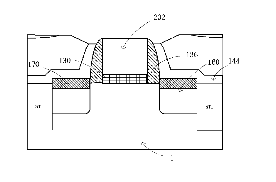
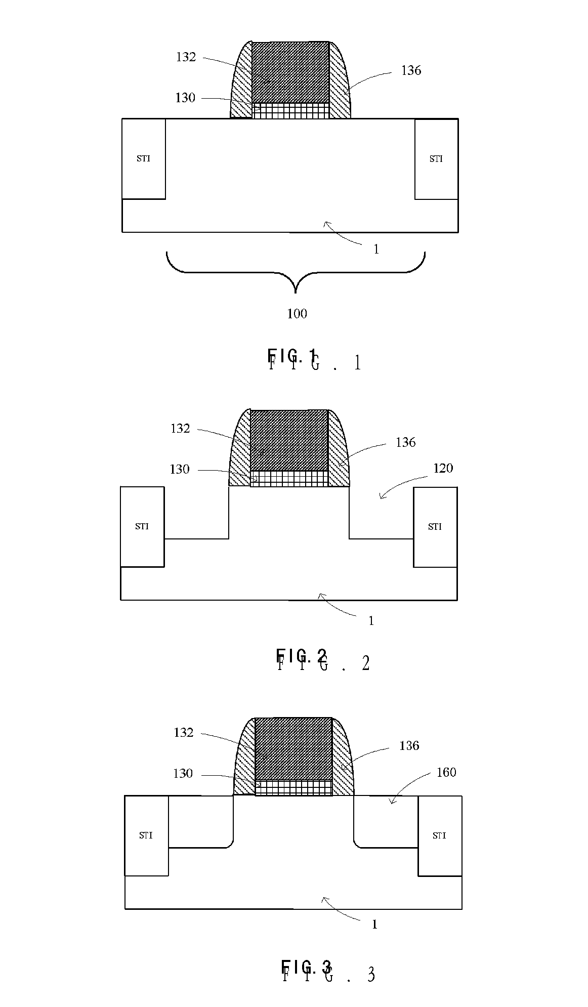
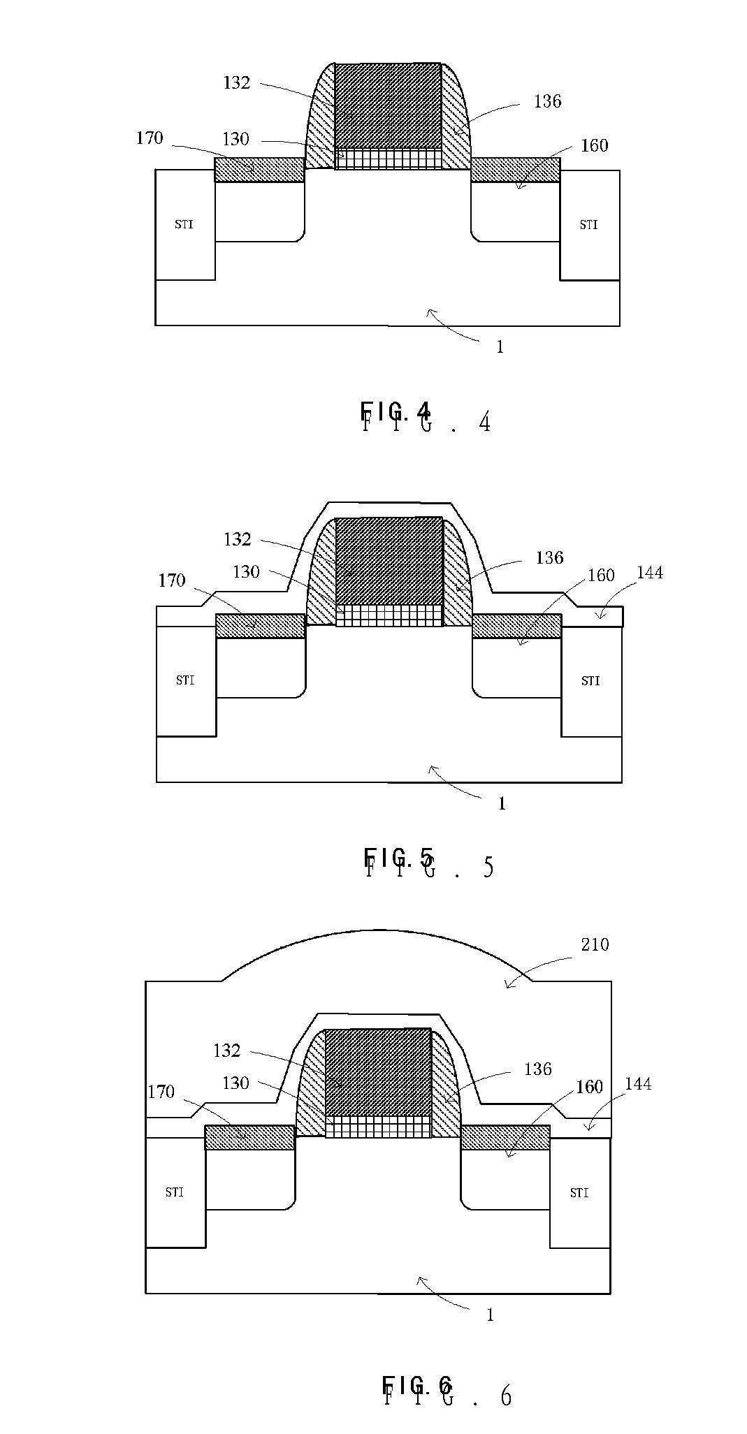
[0035]One or more aspects of the embodiment of the present invention will be described below with reference to the figures, wherein throughout the figures, the same elements are usually represented by the same reference signs. In the descriptions below, many specific details are elucidated for the purpose of explanation, so that a thorough understanding of one or more aspects of the embodiment of the present invention can be provided. However, it is obvious to those skilled in the art that one or more aspects of the embodiment of the present invention may be implemented by said specific details of a lower degree.

[0036]In addition, although specific features or aspects of the embodiment are disclosed with respect to only one preferred embodiment among some preferred embodiments, such features or aspects can be combined with one or more other features or aspects of other preferred embodiments that might be desirable for and advantageous to any given or specific application.

[0037]An ex...


PUM


Abstract

A semiconductor device manufacturing method, comprising: providing a semiconductor substrate, on which a gate conductor layer as well as a source region and a drain region positioned on both sides of the gate conductor layer are provided, forming an etch stop layer on the semiconductor substrate, forming an LTO layer on the etch stop layer, chemical mechanical polishing the LTO layer, forming an SOG layer on the polished LTO layer, the etch stop layer, LTO layer and SOG layer forming a front metal insulating layer, back etching the SOG layer and etch stop layer of the front metal insulating layer to expose the gate conductor layer, and removing the gate conductor layer.

Description

FIELD OF THE INVENTION[0001]The present invention relates to a semiconductor device manufacturing method, in particular to a semiconductor device manufacturing method employing a gate-last process.BACKGROUND OF THE INVENTION[0002]Polysilicon gates prevent further improvement of the performance of metal oxide semiconductor (MOS) devices when the size of the devices is continuously reduced, due to the excessive large resistance of the gates, polysilicon depletion effect and boron penetration effect in PMOS transistors. Meanwhile, a serious interface defect is usually formed when integrating a polysilicon gate with a high K gate dielectric, which results in a pinning phenomenon of the device threshold and reduction in carrier mobility in channel. Therefore, a gate structure is put forward in which a metal gate is used to replace the polysilicon gate.[0003]In an MOS device, the processes of integrating a metal gate / high K gate stack include a gate-first process and a gate-last process. ...

Claims


Application Information

Patent Timeline
IPC IPC(8): H01L21/306
CPCH01L21/31053H01L21/823807H01L21/31055H01L29/66545H01L21/28079H01L21/28088H01L21/31116
Inventor YIN, HUAXIANGXU, QIUXIAMENG, LINGKUANCHEN, DAPENG
Owner INST OF MICROELECTRONICS CHINESE ACAD OF SCI
Why Eureka
Eureka Blog
Learn More