

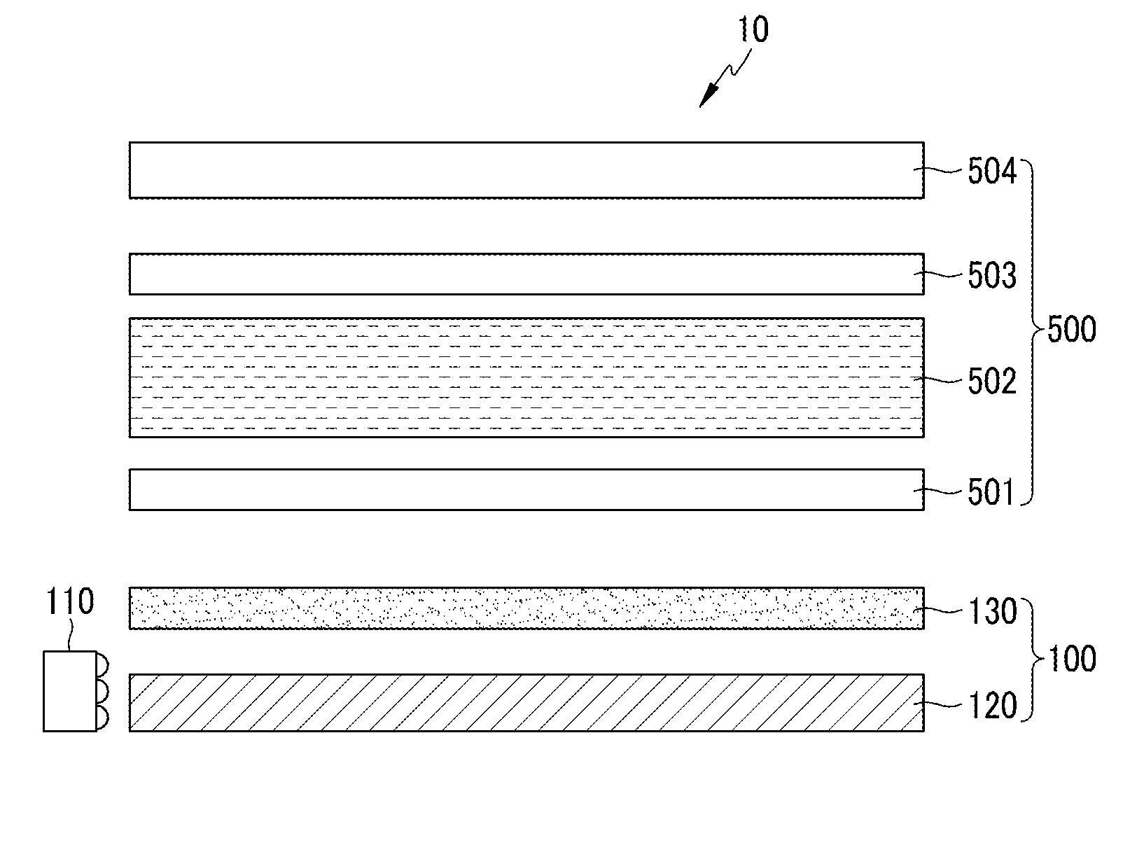
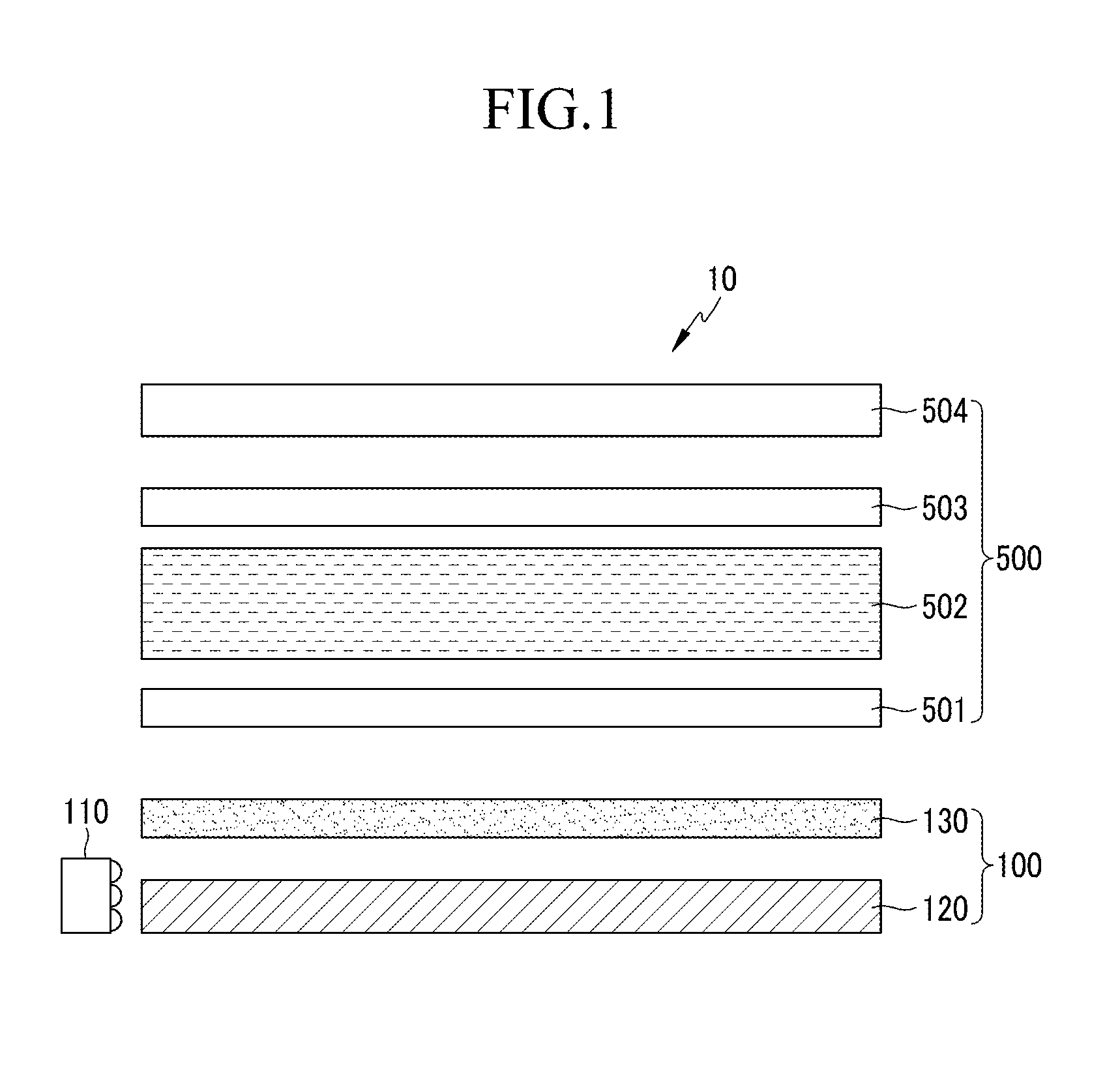
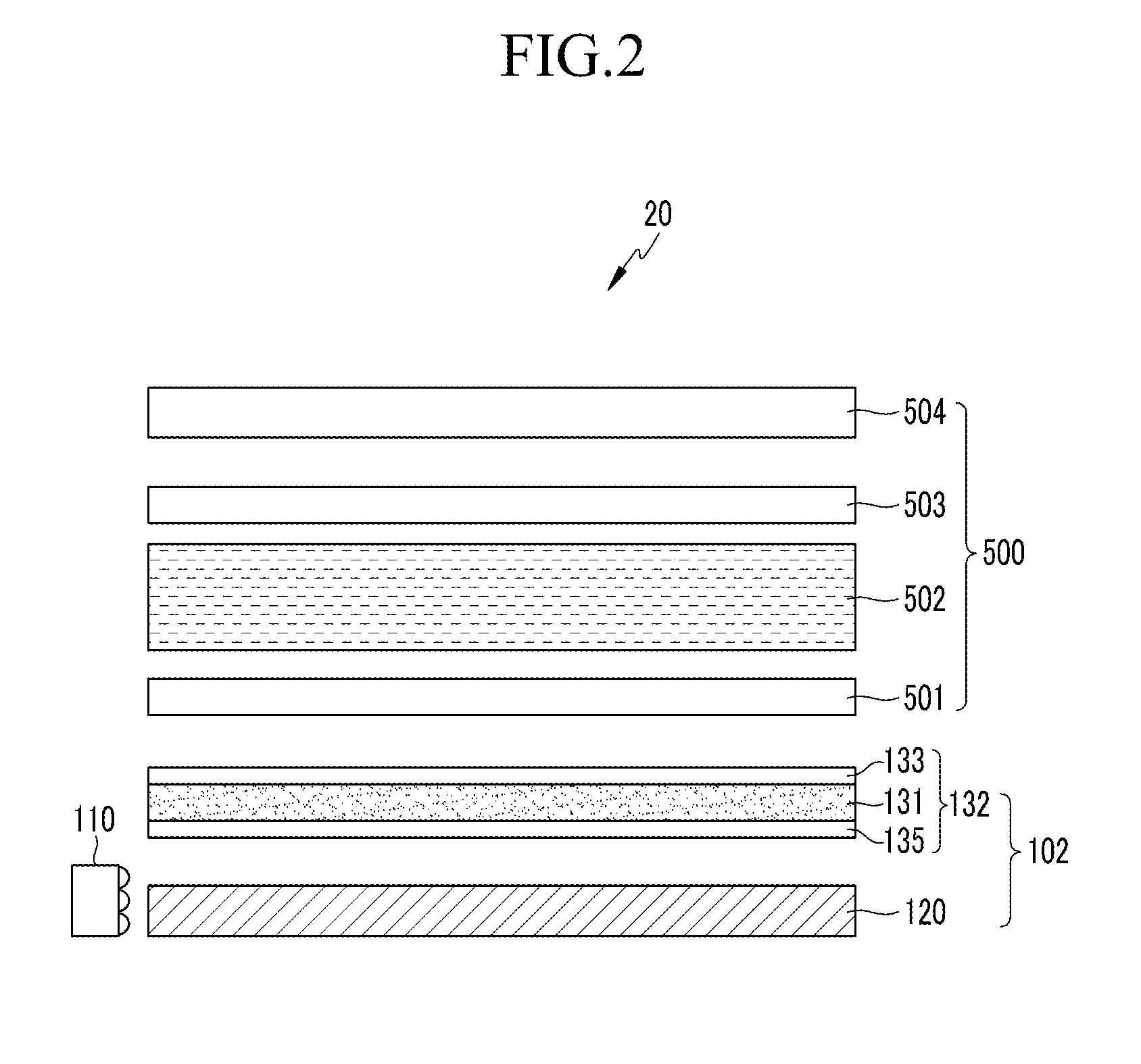
Backlight unit and liquid crystal display including the same
a liquid crystal display and backlight unit technology, applied in the field of backlight units and liquid crystal display devices, can solve the problems of color purity deterioration, difficult to provide desirable uniform luminance of light supplied from the ccfl, and the backlight unit which uses the three color leds as the light source is more expensiv
- Summary
- Abstract
- Description
- Claims
- Application Information
AI Technical Summary
Benefits of technology
Problems solved by technology
Method used
Image

Examples
example 1
Fabrication of Light Conversion Layer
[0175]Green semiconductor nanocrystal (CdSe / ZnS / CdZnS) with a light emitting wavelength of 536 nanometers (nm) is dispersed into 119 microliters (μL) of toluene to have an optical density (“OD”) of 0.10, wherein the optical density is determined using the absorbance of the first absorption maximum wavelength in a UV-Vis absorption spectrum of a 100 times-diluted solution, to provide a green semiconductor nanocrystal dispersion solution.
[0176]Red semiconductor nanocrystal (CdSe / CdSZnS) having a light emitting wavelength of 624 nm is dispersed into 36 μL of toluene to have an optical density (“OD”) of 0.10, to provide a red semiconductor nanocrystal dispersion solution.
[0177]The green semiconductor nanocrystal dispersion and red semiconductor nanocrystal dispersion are mixed, ethanol is added thereto, and then the mixture is centrifuged.
[0178]The supernatant of the solution excluding the centrifuged precipitant is discarded, and the precipitant is ...
example 2
Fabrication of Light Conversion Layer
Synthesis of Green Semiconductor Nanocrystal (InZnP / ZnSeS / ZnS) Coated with Polymer
[0187]4 g of a polyethylene-co-polyacrylic acid copolymer (15 wt % of polyacrylic acid) is put into a flask and 38 mL of toluene is added under a nitrogen atmosphere to prepare a polymer solution. The polymer solution is heated at 120° C. to dissolve the copolymer completely.
[0188]Green semiconductor nanocrystal with a light emitting wavelength of 542 nm is dispersed into 40 mL of toluene to have an optical density (“OD”) of 0.015 (determined using the absorbance of the first absorption maximum wavelength in UV-Vis absorption spectrum of a 100 times-diluted solution), to provide a green semiconductor nanocrystal dispersion solution.
[0189]The green semiconductor nanocrystal dispersion solution is mixed with the polymer solution and stirred at 120° C. for 30 minutes. 10 mL of a solution including diethyl zinc (Zn(Et)2) dissolved in toluene at a concentration of 0.2 mo...
PUM
| Property | Measurement | Unit |
|---|---|---|
| Width | aaaaa | aaaaa |
| Absorbance | aaaaa | aaaaa |
| Wavelength | aaaaa | aaaaa |
Abstract
Description
Claims
Application Information