Organic optoelectronic devices with surface plasmon structures and methods of manufacture

a technology of organic optoelectronic devices and surface plasmons, which is applied in the direction of thermoelectric devices, sustainable manufacturing/processing, and final product manufacturing, etc., can solve the problems of ood being a major cause of device degradation, reliance on indium tin oxide (“ito”) remains a key limiting factor in the design and performance of opvs and other organic optoelectronic devices, and ood is a major

Inactive Publication Date: 2013-06-20
KAMINSKA BOZENA +2
View PDF11 Cites 27 Cited by
  • Summary
  • Abstract
  • Description
  • Claims
  • Application Information

AI Technical Summary

Benefits of technology

[0006]In accordance with a first aspect, an organic optoelectronic device is disclosed. The organic optoelectronic device includes a carrier substrate, a metal anode electrode layer disposed at least partially on the carrier substrate, an organic electronic active region including one or more organic layers and disposed at least partially on the metal anode electrode layer, and a cathode electrode layer disposed at least partially on the organic photoactive layer. The metal anode electrode layer includes periodic arrays of sub-wavelength nanostructures.

Problems solved by technology

Nevertheless, a reliance on indium tin oxide (“ITO”) remains a key limiting factor in the design and performance of OPVs and other organic optoelectronic devices (“OODs”).
ITO as a transparent conductor is known to have several disadvantages and design and performance constraints.
First, ITO as used in an OOD is a major cause of device degradation.
ITO has a tendency to crack or break when deposited on flexible substrates and subjected to bending.
The formation and propagation of cracks in the ITO in turn increase its electrical resistance, resulting in a loss of conductivity.
ITO tends to degrade over time, permitting oxygen and moisture to diffuse into the organic layers of the OOD and adversely affecting the DOD's operational lifetime.
A further disadvantage of ITO is cost.
ITO requires indium, which due to scarcity has high material cost that prevents the wide deployment of ITO in cost-conscious industries, such as in the OPV industry.
ITO also suffers from the compromise between conductivity and transparency.
During ITO film deposition, the high concentration of charge carriers increases the conductivity of the ITO, but decreases its transparency, which is undesirable, as OODs typically require both high anode conductivity and transparency to deliver optimal device performance.
Although transparent films of carbon nanotubes or highly conductive polymers have been proposed as replacements to ITO, the performance of OPVs and other OODs have not been substantially enhanced to date as a result.

Method used


Image

  • Organic optoelectronic devices with surface plasmon structures and methods of manufacture
  • Organic optoelectronic devices with surface plasmon structures and methods of manufacture
  • Organic optoelectronic devices with surface plasmon structures and methods of manufacture

Examples


Embodiment Construction

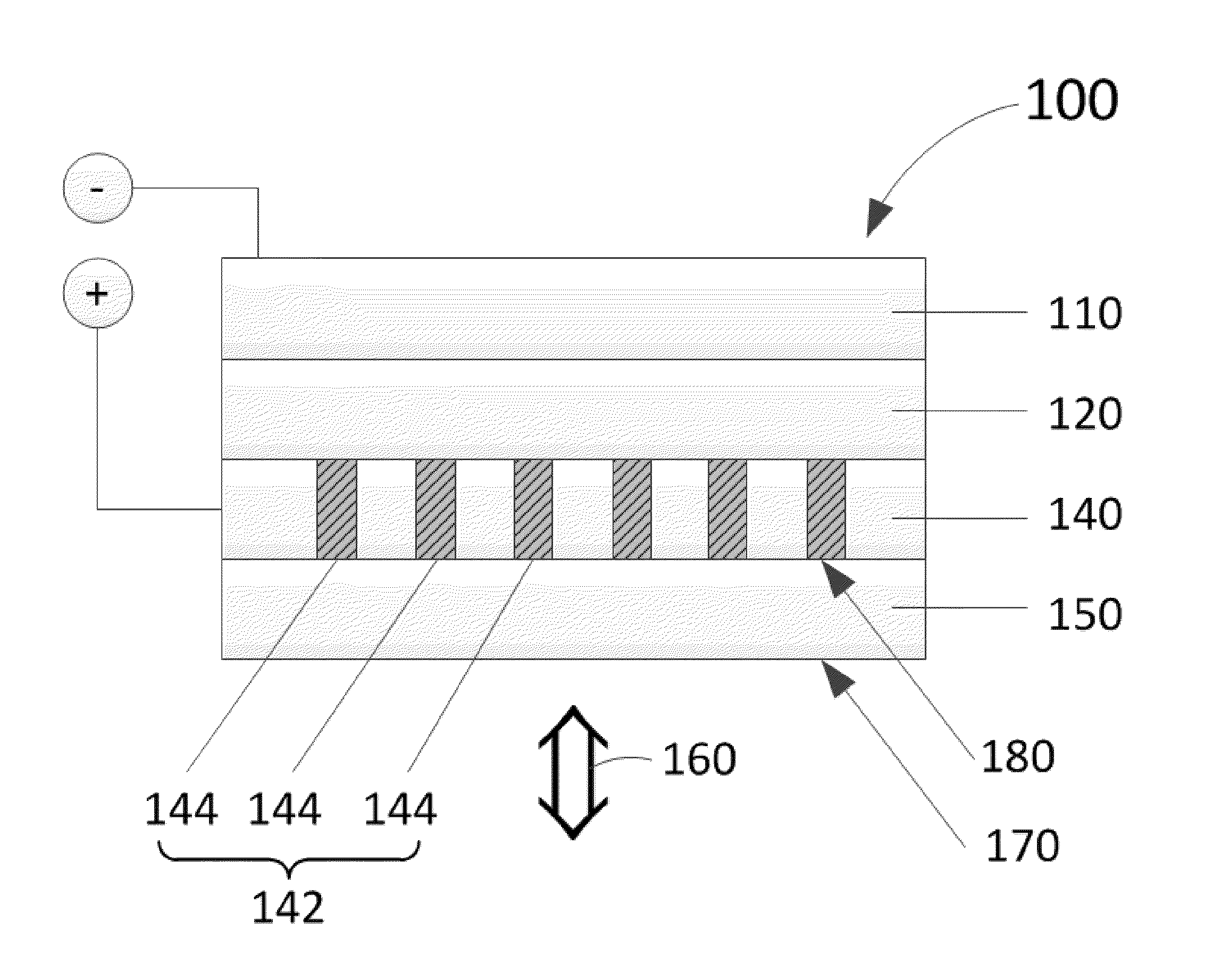
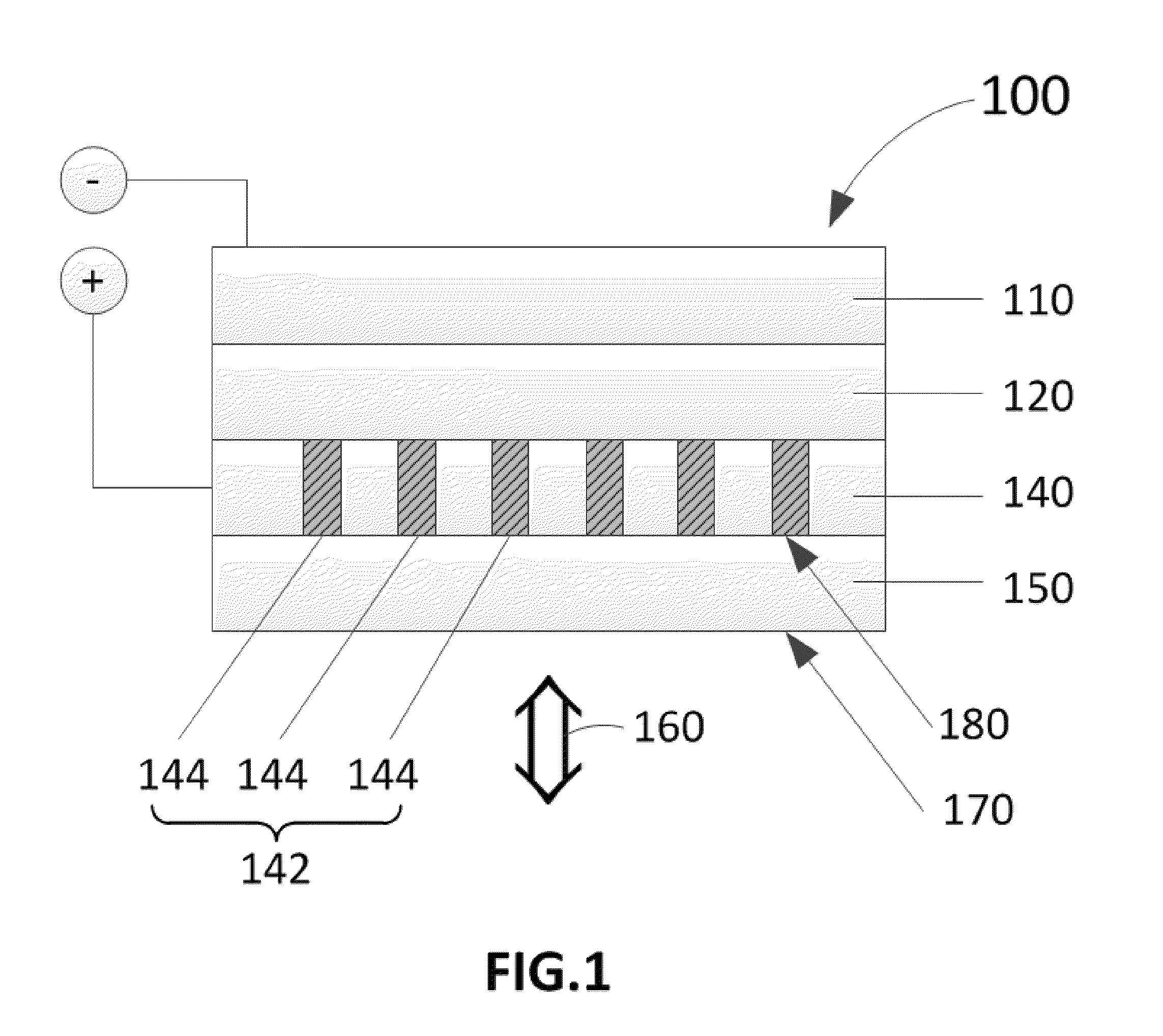
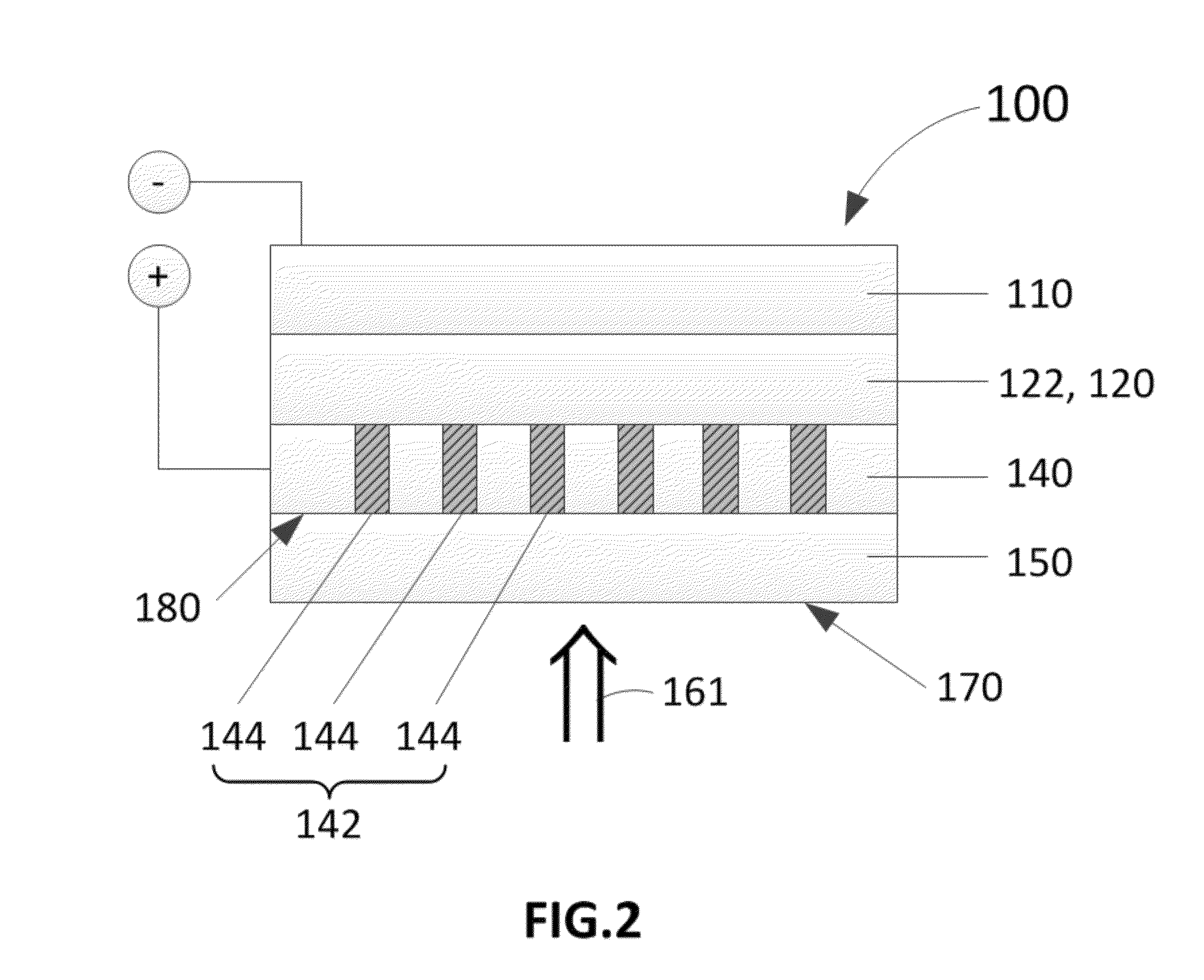
[0038]In one embodiment of the present invention, an ordered or periodic array of sub-wavelength nanostructures is optimally formed in a metal layer, such as an exemplary metallic foil or film, for use as an anode in an organic optoelectronic device (“OOD”), such as in an organic photovoltaic device (“OPV”) or an organic light emitting diode device (“OLED”), for example. The metal anode layer comprising one or more nanostructures may be desirably adapted for use in an OOD as a replacement or alternative to a conventional high work function, optically-transmissive front electrode, which is typically made of indium tin oxide (“ITO”). As compared to conventional ITO-OODs, the ITO-free OOD configuration of the present invention leverages the relatively higher conductivity of metal as the anode materials (e.g. silver (Ag), gold (Au), and copper (Cu)), and the Surface Plasmonic (“SP”) and Extraordinary Optical Transmission (“EOT”) properties observed in the perforated metal anode electrod...


PUM


Abstract

An organic optoelectronic device is disclosed. The organic optoelectronic device includes a carrier substrate, an anode electrode layer disposed at least partially on the carrier substrate, an organic electronic active region including one or more organic layers and disposed at least partially on the anode electrode layer, and a cathode electrode layer disposed at least partially on the organic photoactive layer. The anode electrode layer has a periodic array of sub-wavelength nanostructures. Methods of manufacturing an organic optoelectronic device are also disclosed.

Description

1. TECHNICAL FIELD[0001]The present invention relates generally to organic optoelectronic devices, and more particularly, to organic optoelectronic devices with surface plasmonic structures to enhance their performance and / or their methods of manufacture.2. Background of the Invention[0002]Research in bulk heterojunction (“BHJ”) structures has led to the development of organic photovoltaics devices (“OPVs”) with efficiency close to 9%. Nevertheless, a reliance on indium tin oxide (“ITO”) remains a key limiting factor in the design and performance of OPVs and other organic optoelectronic devices (“OODs”).[0003]ITO as a transparent conductor is known to have several disadvantages and design and performance constraints. First, ITO as used in an OOD is a major cause of device degradation. ITO has a tendency to crack or break when deposited on flexible substrates and subjected to bending. The formation and propagation of cracks in the ITO in turn increase its electrical resistance, resul...

Claims


Application Information

Patent Timeline
Patent Type & Authority Applications(United States)
IPC IPC(8): H01L51/50H01L31/18H01L51/40B82Y30/00
CPCB82Y30/00Y02E10/549B82Y20/00H01L51/5206H01L51/441H10K30/81H10K50/81Y02P70/50H10K50/813
Inventor KAMINSKA, BOZENAOMRANE, BADRLANDROCK, CLINTON K.
Owner KAMINSKA BOZENA
Why Eureka
Try Eureka