Integrated MEMS device

a mems device and integrated technology, applied in the direction of electrical transducers, loudspeakers, semiconductor electrostatic transducers, etc., can solve the problems of high packaging cost and other problems, and achieve the effects of low manufacturing cost, high reliability and high reliability

Inactive Publication Date: 2013-06-27
WINDTOP TECH CORP
View PDF5 Cites 126 Cited by
  • Summary
  • Abstract
  • Description
  • Claims
  • Application Information

AI Technical Summary

Benefits of technology

[0006]Another object of the present invention is to provide a MEMS microphone having high reliability and low manufacturing cost.
[0007]Yet another object of the present invention is to provide a MEMS pressure sensor having high reliability and low manufacturing cost.

Problems solved by technology

The problem with the two-chip solutions using wire bonding is that the wire is basically an inductive antenna and can pickup high frequency noise whose harmonics at low frequency band interferes with the sound in its frequency range.
The problem with the above mentioned single-chip with metal composite film as diaphragm is long term reliability concern due to film instability when gone through temperature cycles.
The other drawbacks of the above methods are high cost due to packaging.

Method used


Image

  • Integrated MEMS device
  • Integrated MEMS device
  • Integrated MEMS device

Examples


Embodiment Construction

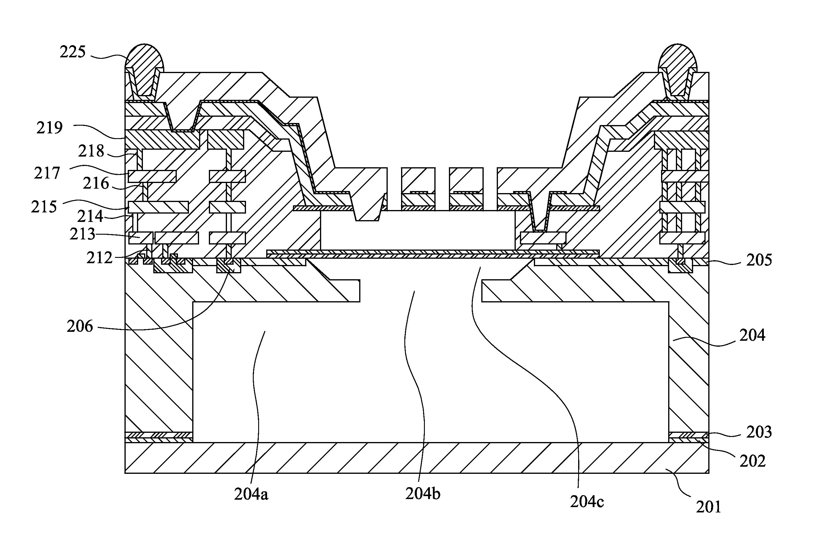
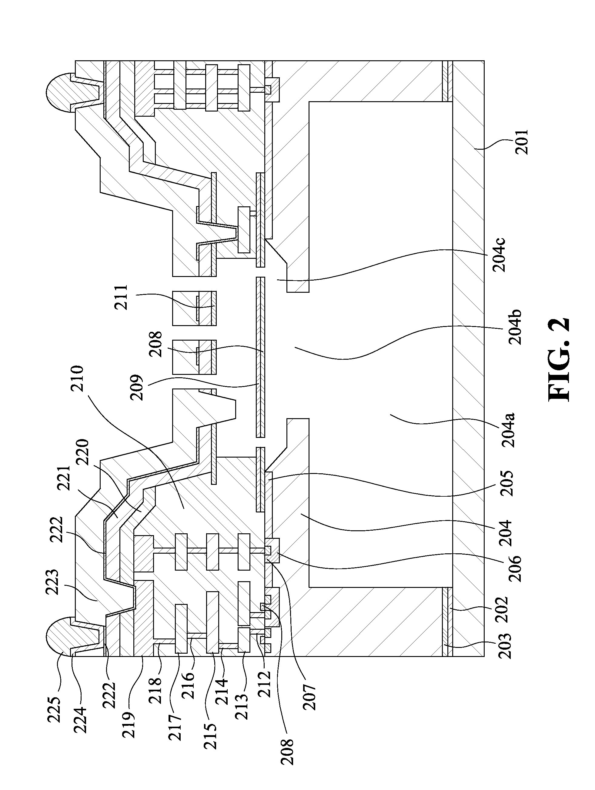
[0021]FIG. 2 shows a cross-sectional view of an exemplary embodiment of a MEMS device having a single chip structure fabricated to function as a MEMS microphone according to the present invention. As shown in FIG. 2, the integrated MEMS microphone of the present invention combines ASIC and MEMS and uses flip chip package and wafer bonding technology to fabricate. From the bottom up, the structure of an integrated MEMS microphone of the present invention includes a bonding wafer layer 201, a bonding layer 202, an aluminum layer 203, a CMOS substrate layer 204 defining, from the bottom up, a large back chamber area (LBCA) 204a, a small back chamber area (SBCA) 204b and a sound damping path (SDP) 204c, a field oxide (FOX) layer 205, a first set of implant doped silicon areas 206, a second set of implant doped silicon areas 207, a first polysilicon layer 208, a second polysilicon layer 209, said first polysilicon layer 208 and said second polysilicon layer 209 forming a bottom plate, an...


PUM


Abstract

An integrated MEMS device is provided, including, from bottom up, a bonding wafer layer, a bonding layer, an aluminum layer, a CMOS substrate layer defining a large back chamber area (LBCA), a small back chamber area (SBCA) and a sound damping path (SDP), a set of CMOS wells, a field oxide (FOX) layer, a set of CMOS transistor sources / drains, a first polysilicon layer forming CMOS transistor gates, a second polysilicon layer, said CMOS wells, said CMOS transistor sources / drains and said CMOS gates forming CMOS transistors, an oxide layer embedded with a plurality of metal layers interleaved with a plurality of via hole layers, and a gap control layer, an oxide layer, a first Nitride deposition layer, a metal deposition layer, a second Nitride deposition layer, an under bump metal (UBM) layer made of preferably Al / NiV / Cu and a plurality of solder spheres.

Description

FIELD OF THE INVENTION[0001]The present invention generally relates to an integrated MEMS device, and more specifically to an integrated MEMS device built with CMOS process, Flip Chip package and wafer bonding technology.BACKGROUND OF THE INVENTION[0002]MEMS devices have long been attracting attentions due to a wide range of portable applications. For example, MEMS microphone has recently gained attraction due to the use of portable devices such as smart phones, tablet and notebook computers. Also, widely used are in the devices which require noise cancellation due to the MEMS microphone device-device uniformity. However, most of the MEMS microphone was made with separate MEMS sensors and ASIC circuits with the final products assembled by wire bonding on top of a PCB substrate. Some MEMS microphones were made with single chip without wire bonding using top metal film as MEMS diaphragms.[0003]FIG. 1 shows a schematic view of a conventional structure of a MEMS microphone with two-chip...

Claims


Application Information

Patent Timeline
Patent Type & Authority Applications(United States)
IPC IPC(8): H01L27/20
CPCB81C2203/0771B81C1/00246B81B2201/0257B81B2207/015H04R19/04B81C2203/0742H04R19/005H04R31/00H04R2201/003B81C2203/0714H01L2224/48137H01L2224/8592H01L2224/48091H01L2224/48227H01L2924/00014
Inventor CHEN, KUN-LUNG
Owner WINDTOP TECH CORP
Why Eureka
Try Eureka