Combinatorial Processing Using High Deposition Rate Sputtering

a sputtering and sputtering technology, applied in the direction of chemical vapor deposition coating, vacuum evaporation coating, coating, etc., can solve the problems of significant contamination, poor film quality, and low deposition rate, and achieve the effect of minimizing the sputtering gap and high deposition rate of sputtering

Inactive Publication Date: 2013-07-04
INTERMOLECULAR
View PDF4 Cites 6 Cited by
  • Summary
  • Abstract
  • Description
  • Claims
  • Application Information

AI Technical Summary

Benefits of technology

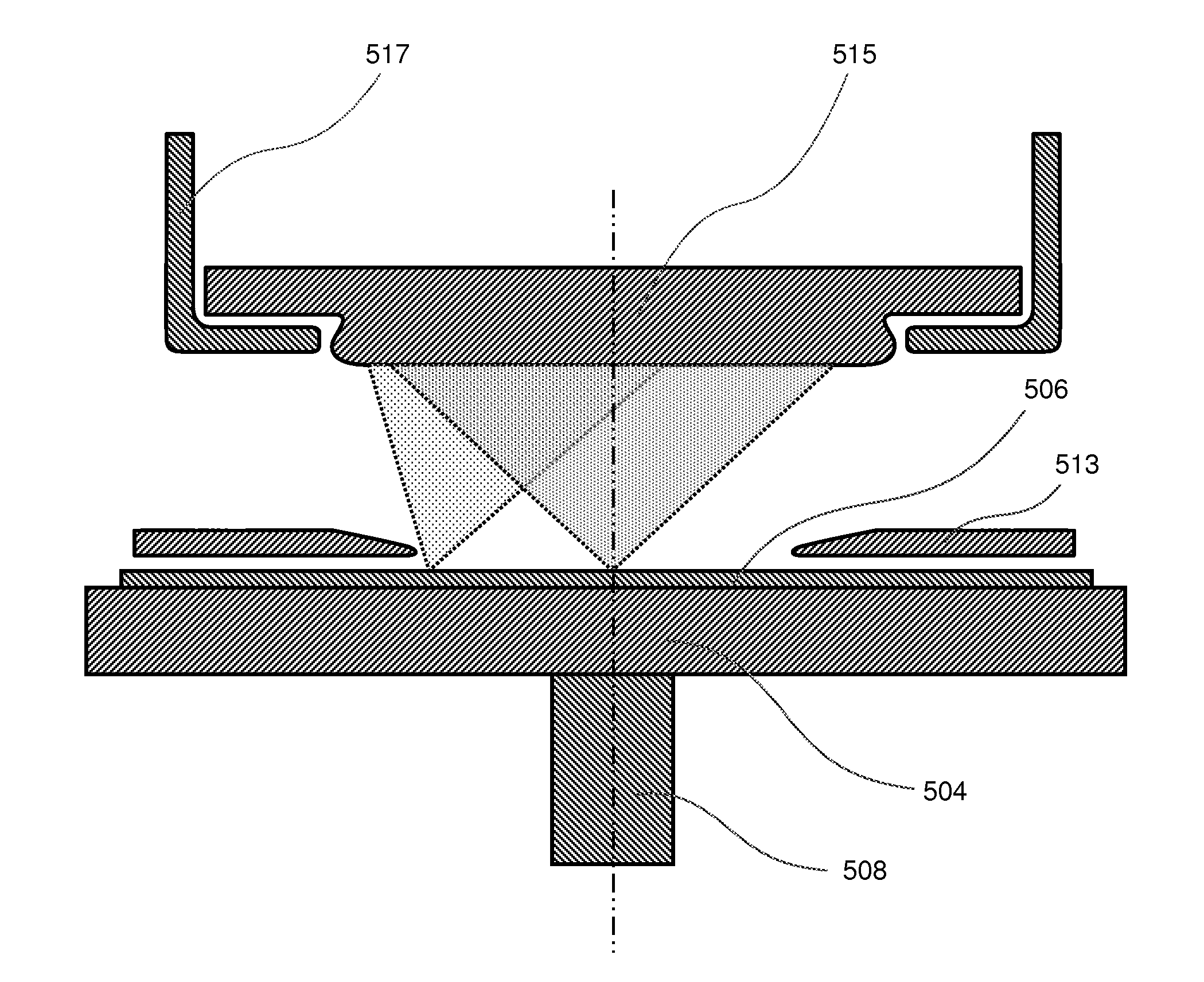
[0007]Embodiments of the present invention provide apparatuses for combinatorial processing using high-deposition-rate sputtering for depositing layers onto a substrate. A high deposition rate of sputtering is provided by locating the sputtering source much closer to the substrate than is practiced in prior art deposition methods. The apparatuses generally comprise a process chamber; one or more sputtering sources disposed within the process chamber; a substrate support operable to support a substrate; a shield positioned between the sputtering sources and the substrate, the shield comprising an aperture positioned under each sputtering source; and a transport system connected to the substrate support capable of positioning the substrate such that one of a plurality of site-isolated regions on the substrate can be exposed to sputtered material through the aperture positioned under each of the sputtering sources. Each sputtering source comprises a sputtering target, and the spacing between the sputtering target and the substrate is less than 100 mm.
[0008]The apparatus is operable to vary one or more process parameters comprising one or more sputtering parameters, sputtering atmosphere parameters, substrate parameters, or combinations thereof. The process parameters can be varied in a combinatorial manner among the plurality of site-isolated regions. The sputtering parameters typically comprise exposure times, power, sputtering target material, target-to-substrate spacing, or combinations thereof. The sputtering atmosphere parameters comprise total pressure, carrier gas composition, carrier gas flow rate, reactive gas composition, reactive gas flow rate, or combinations thereof. The reactive gas flow rate can be greater than or equal to zero in order to vary the reactive gas composition in an inert carrier gas. The substrate parameters comprise substrate material, surface condition, substrate temperature, substrate bias, or combinations thereof. The sputtering source is oriented approximately normal to the substrate so that the sputtering gap is minimized while providing uniform sputtering to all portions of the site-isolated region on the substrate. In some embodiments, the sputtering gap is between about 20 mm and about 100 mm. In some embodiments, the sputtering gap is between about 50 mm and about 75 mm.
[0009]The apparatus can further comprise an aperture shutter for each aperture, wherein the aperture shutter is moveably disposed over the aperture. The substrate support is capable of providing independent substrate temperature control and applying a bias voltage. The apparatus can further comprise a plurality of sputtering sources, such as two, three, four, five, or six sputtering sources. The apertures typically have an opening smaller than the substrate so that a plurality of discrete regions of the substrate can be subjected to distinct process conditions in a combinatorial manner.
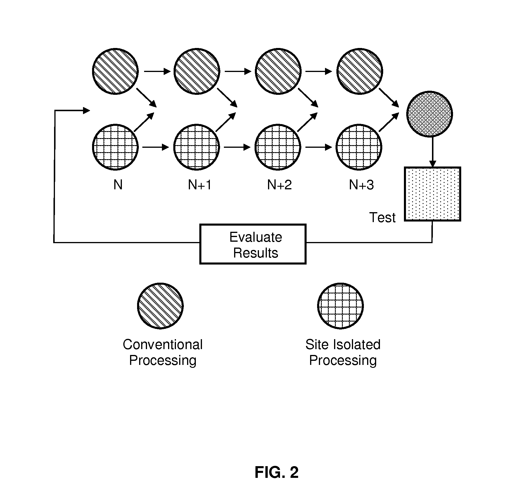
[0010]Embodiments of the present invention also include methods of depositing layers on a substrate in a combinatorial manner. The methods generally comprise exposing a first site-isolated region of a surface of a substrate to material from a sputtering source under a first set of process conditions, and exposing a second site-isolated region of a surface of the substrate to material from a sputtering source under a second set of process conditions. During exposure of the surface of the substrate to the sputtering source, the remaining area of the substrate is not exposed to the material from the sputtering target, enabling site-isolated deposition of sputtered material onto the substrate. The method can further comprise exposing three or more site-isolated regions of the substrate to material from a sputtering source under distinct sets of process conditions.

Problems solved by technology

However, deposition rates can suffer.
Significant contamination and poor film quality are common byproducts of long processing time.

Method used


Image

  • Combinatorial Processing Using High Deposition Rate Sputtering
  • Combinatorial Processing Using High Deposition Rate Sputtering
  • Combinatorial Processing Using High Deposition Rate Sputtering

Examples


Embodiment Construction

[0017]Before the present invention is described in detail, it is to be understood that unless otherwise indicated this invention is not limited to specific layer compositions or surface treatments. It is also to be understood that the terminology used herein is for the purpose of describing particular embodiments only and is not intended to limit the scope of the present invention.

[0018]It must be noted that as used herein and in the claims, the singular forms “a,”“and” and “the” include plural referents unless the context clearly dictates otherwise. Thus, for example, reference to “a layer” includes two or more layers, and so forth.

[0019]Where a range of values is provided, it is understood that each intervening value, to the tenth of the unit of the lower limit unless the context clearly dictates otherwise, between the upper and lower limit of that range, and any other stated or intervening value in that stated range, is encompassed within the invention. The upper and lower limits...


PUM

PropertyMeasurementUnit
diameteraaaaaaaaaa
diameteraaaaaaaaaa
bias voltageaaaaaaaaaa

Abstract

Apparatuses and methods for high-deposition-rate sputtering for depositing layers onto a substrate are disclosed. The apparatuses generally comprise a process chamber; one or more sputtering sources disposed within the process chamber, wherein each sputtering source comprises a sputtering target; a substrate support disposed within the process chamber; a shield positioned between the sputtering sources and the substrate, the shield comprising an aperture positioned under each sputtering source; and a transport system connected to the substrate support capable of positioning the substrate such that one of a plurality of site-isolated regions on the substrate can be exposed to sputtered material through the aperture positioned under each of the sputtering sources; wherein the spacing between the sputtering target and the substrate is less than 100 mm. The apparatus enables high deposition rate sputtering onto site-isolated regions on the substrate.

Description

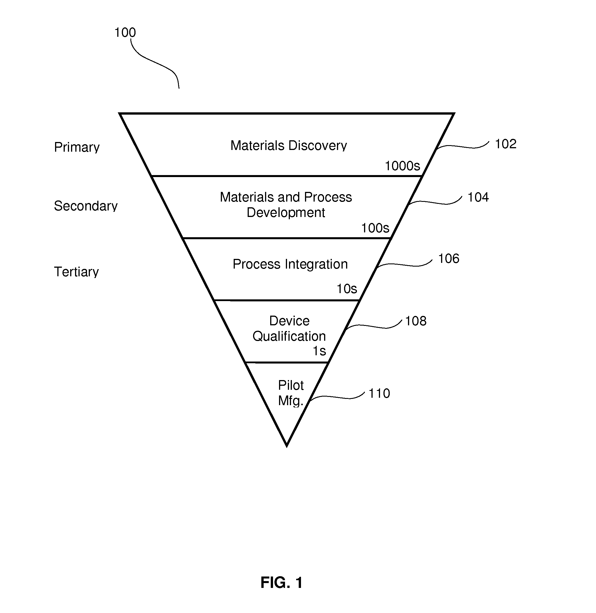
CROSS REFERENCE TO RELATED APPLICATION[0001]This application is related to co-owned U.S. patent application Ser. No. 13 / 281,316 entitled “High Metal Ionization Sputter Gun,” filed on Oct. 25, 2011, which is incorporated herein by reference.FIELD OF THE INVENTION[0002]One or more embodiments of the present invention relate to methods and apparatuses for combinatorial processing using high rate of sputter deposition of thin films.BACKGROUND[0003]Physical vapor deposition (PVD) is commonly used within the semiconductor industry as well as within solar, glass coating, and other industries, in order to deposit a layer over a substrate. Sputtering is a common physical vapor deposition method, where atoms or molecules are ejected from a target material by high-energy particle bombardment and then deposited onto the substrate.[0004]In order to identify different materials, evaluate different unit process conditions or parameters, or evaluate different sequencing and integration of processes...

Claims


Application Information

Patent Timeline
Patent Type & Authority Applications(United States)
IPC IPC(8): C23C14/34
CPCC23C14/3464C23C14/044
Inventor YANG, HONG SHENGHONG, ZHENDONGLANG, CHI-I
Owner INTERMOLECULAR
Why Eureka
Try Eureka