
Localized surface plasmon resonance sensor using chalcogenide materials and method for manufacturing the same

a technology of chalcogenide and localized surface plasmon, which is applied in the field of can solve the problems of difficult modification of the structure of precious metal materials, difficult to detect biomarkers with existing localized surface plasmon resonance sensors using precious metals, and complicated doping process

Inactive Publication Date: 2013-07-04
KOREA INST OF SCI & TECH
View PDF1 Cites 4 Cited by
  • Summary
  • Abstract
  • Description
  • Claims
  • Application Information

AI Technical Summary

Benefits of technology

The patent describes a method for making a sensor that detects infrared light using a layer called LSPR. This method allows for easy patterning of the LSPR layer using a laser, instead of the complicated and expensive process of lithography. The composition of the material used to make the LSPR layer can be controlled to change the carrier density, and the sensor can operate in the infrared region. Overall, this method simplifies the process of making the sensor and allows for better control over its properties.

Problems solved by technology

But, since the wavelength allowing detection of the biomarkers is usually in the mid-infrared region, there is difficulty in detecting the biomarkers with the existing localized surface plasmon resonance sensors using precious metals.
However, the modification of the structure of the precious metal materials is not easy and it is much more favorable to choose other materials that operate well in the infrared region in terms of cost.
But, the doping process is complicated.
However, since these top-down processes are complicated and expensive, they are not suited for applications where a lot of inexpensive sensors are required such as biological or ecological detection.
Although bottom-up type self-assembling processes are attempted to overcome this problem, it is difficult to obtain the desired patterns accurately.

Method used


Image

  • Localized surface plasmon resonance sensor using chalcogenide materials and method for manufacturing the same
  • Localized surface plasmon resonance sensor using chalcogenide materials and method for manufacturing the same
  • Localized surface plasmon resonance sensor using chalcogenide materials and method for manufacturing the same

Examples


Embodiment Construction

[0020]Hereinafter, embodiments of the present disclosure will be described in detail referring to the attached drawings.

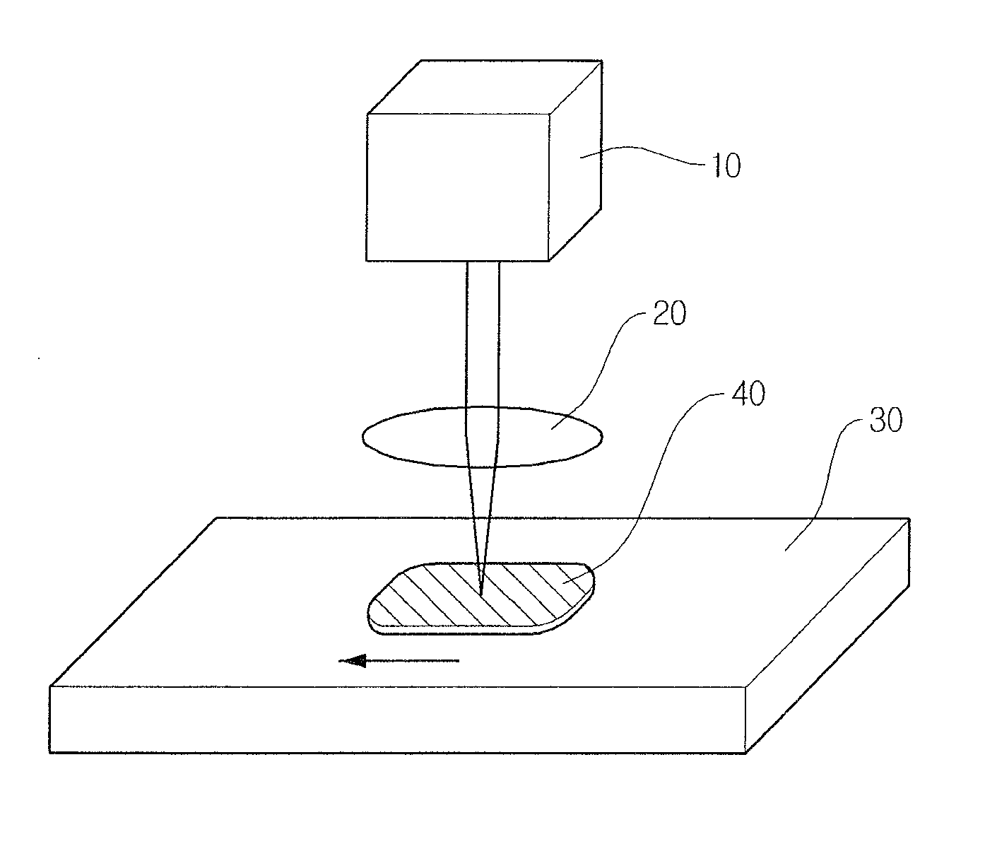
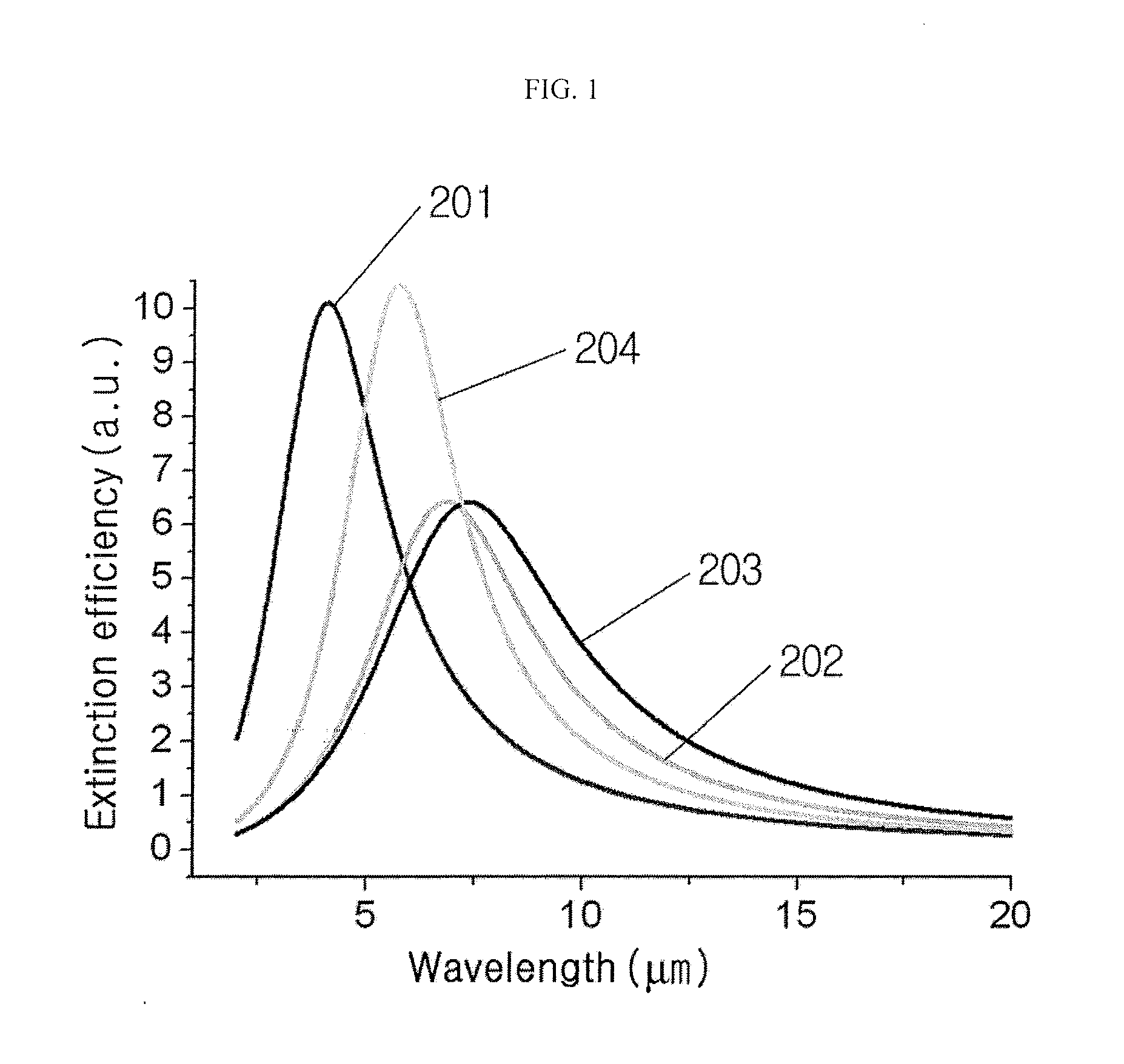
[0021]A localized surface plasmon resonance (LSPR) sensor according to an exemplary embodiment may comprise a light source, an LSPR excitation layer and a detector. The light source may irradiate light to the LSPR excitation layer. The LSPR excitation layer generates localized surface plasmons as being excited by incident light of a specific resonance wavelength. As a result, at the resonance wavelength, most of light energy is transferred to free electrons in the LSPR excitation layer. The detector may detect a light absorption signal and / or a light scattering signal by detecting light penetrating the LSPR excitation layer or reflected on the LSPR excitation layer.

[0022]The LSPR phenomenon is characterized by light absorption associated with the resonance and light scattering associated with energy relaxation. Accordingly, the characteristics of the LSPR resonance...


PUM


Abstract

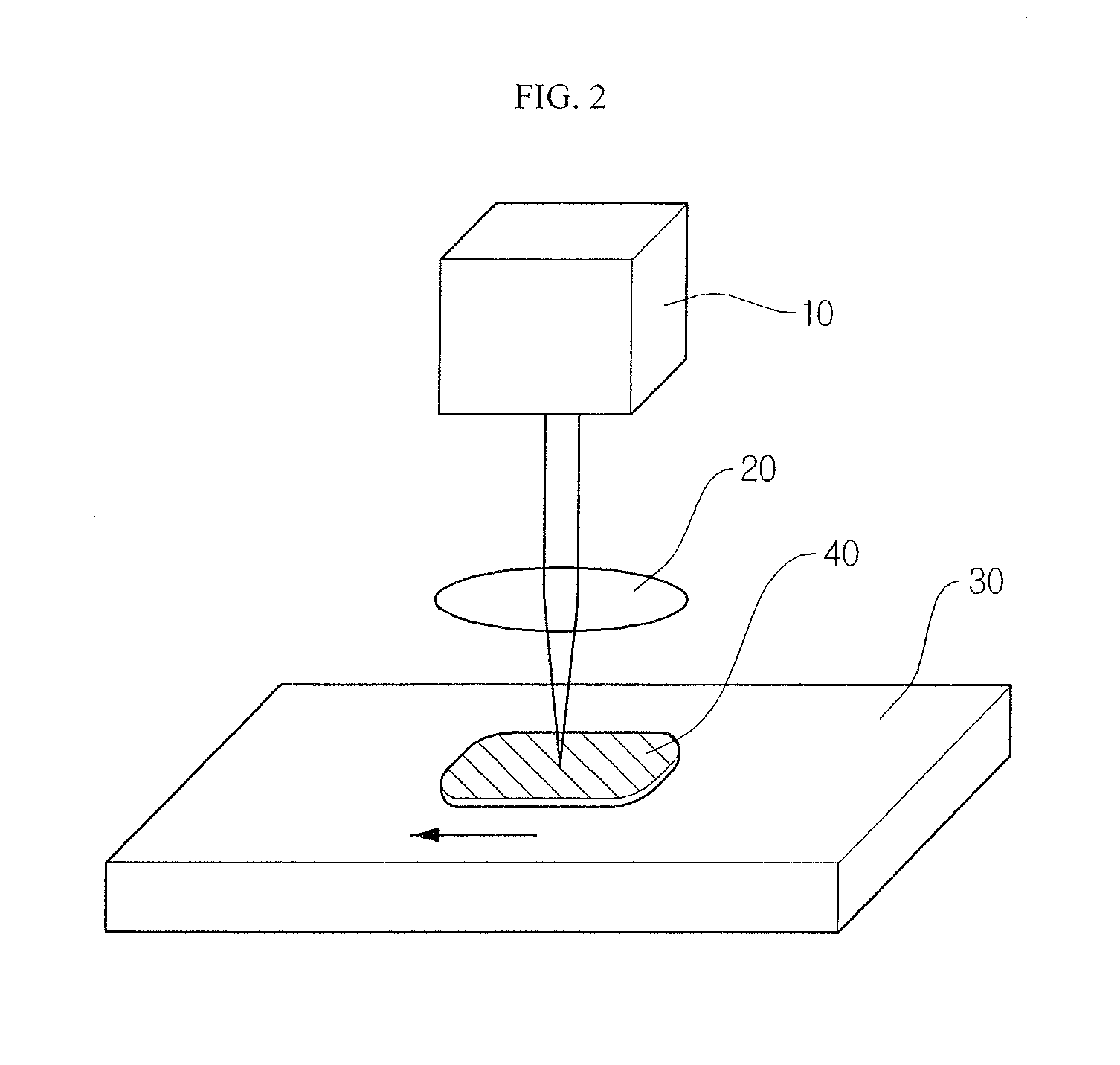
A localized surface plasmon resonance sensor may include a localized surface plasmon excitation layer including a chalcogenide material. The chalcogenide material may include: a first material including at least one of selenium (Se) and tellurium (Te); and a second material including at least one of germanium (Ge) and antimony (Sb). The localized surface plasmon excitation layer may be prepared by forming a thin film including the chalcogenide material and crystallizing the thin film to have a predetermined pattern by irradiating laser on the thin film.

Description

CROSS-REFERENCE TO RELATED APPLICATION[0001]This application claims priority to Korean Patent Application No. 10-2011-0144676, filed on Dec. 28, 2011, and all the benefits accruing therefrom under 35 U.S.C. §119, the contents of which in its entirety are herein incorporated by reference.BACKGROUND[0002]1. Field[0003]Embodiments relate to s localized surface plasmon resonance sensor using a chalcogenide material and a method for manufacturing same.[0004]2. Description of the Related Art[0005]Localized surface plasmon resonance is a phenomenon occurring when a collective oscillation of free electrons in a material is restricted inside a structure whose dimension is smaller than the wavelength of incident light. Since the resonance wavelength at which localized surface plasmons resonance is induced is very sensitively dependent on particle size and shape, change in surrounding medium, or the like, a biochemical sensor that can be utilized in the field of medicine, environment, etc. may...

Claims


Application Information

Patent Timeline
IPC IPC(8): H01L31/032H01L31/18
CPCB82Y15/00G02B5/008H01L31/0324H01L31/186G01N33/54373G01N21/554H01L31/18G01N21/27G01N21/55
Inventor LEE, TAEK SUNGLEE, KYEONG SEOKKIM, IN HOLEE, WOOK SEONGJEONG, DOO SEOKKIM, WON MOKCHEONG, BYUNG KI
Owner KOREA INST OF SCI & TECH
Learn More