Photoresist pattern trimming methods

a technology of photoresist and pattern, applied in the field of electronic device manufacturing, can solve the problems of inability to achieve a good process window for isolated lines and posts through direct lithographic imaging, and the difference in solubility characteristics between exposed and unexposed regions of resist, so as to achieve a significant improvement of the process window for the formation of patterns such as isolated lines and posts

Active Publication Date: 2013-07-04
ROHM & HAAS ELECTRONICS MATERIALS LLC
View PDF3 Cites 54 Cited by
  • Summary
  • Abstract
  • Description
  • Claims
  • Application Information

AI Technical Summary

Benefits of technology

[0009]In accordance with an aspect of the invention, methods of trimming photoresist patterns are provided. The methods comprise, in sequence: (a) providing a semiconductor substrate comprising one or more layers to be patterned on an upper surface thereof; (b) forming a photoresist pattern on the one or more layers to be patterned, wherein the photoresist pattern comprises a plurality of features and is formed from a chemically amplified photoresist composition, the photoresist pattern comprising a matrix polymer having acid labile groups; (c) coating a photoresist trimming composition over the photoresist pattern, wherein the trimming composition comprises a matrix polymer, a thermal acid generator and a solvent, and wherein the trimming composition is free of cross-linking agents; (d) heating the coated semiconductor substrate to generate an acid in the trimming composition from the thermal acid generator, thereby causing a change in polarity of the photoresist matrix polymer in a surface region of the photoresist pattern; and (e) contacting the photoresist pattern with a developing solution to remove the surface region of the photoresist pattern. As a result of methods in accordance with the invention, the process window for formation of patterns such as isolated lines and posts can be significantly improved.

Problems solved by technology

This creates a difference in solubility characteristics between exposed and unexposed regions of the resist in an aqueous alkaline developer solution.
This standard immersion lithography process, however, is generally not suitable for manufacture of devices requiring greater resolution, for example, for the 32 nm and 22 nm half-pitch nodes.
Achieving a good process window for isolated lines and posts through direct lithographic imaging is, however, extremely difficult due to poor aerial image contrast at defocus as compared with dense lines.

Method used


Image

  • Photoresist pattern trimming methods
  • Photoresist pattern trimming methods
  • Photoresist pattern trimming methods

Examples


example 1

PTC 1

[0047]2.813 g copolymer of t-butyl acrylate / methacrylic acid (7 / 3 of mole ratio), 0.087 g of TAG 1, 19.420 g decane and 77.680 g 2-methyl-1-butynol were mixed until all components were dissolved. The resulting mixture was filtered with a 0.2 micron Nylon filter.

example 2

PTC 2

[0048]2.610 g of copolymer of t-butyl acrylate / methacrylic acid (7 / 3 of mole ratio), 0.290 g of TAG 2, 24.275 g decane and 72.825 g 2-methyl-1-butynol were mixed until all components were dissolved. The resulting mixture was filtered with a 0.2 micron Nylon filter.

Lithographic Processing

example 3

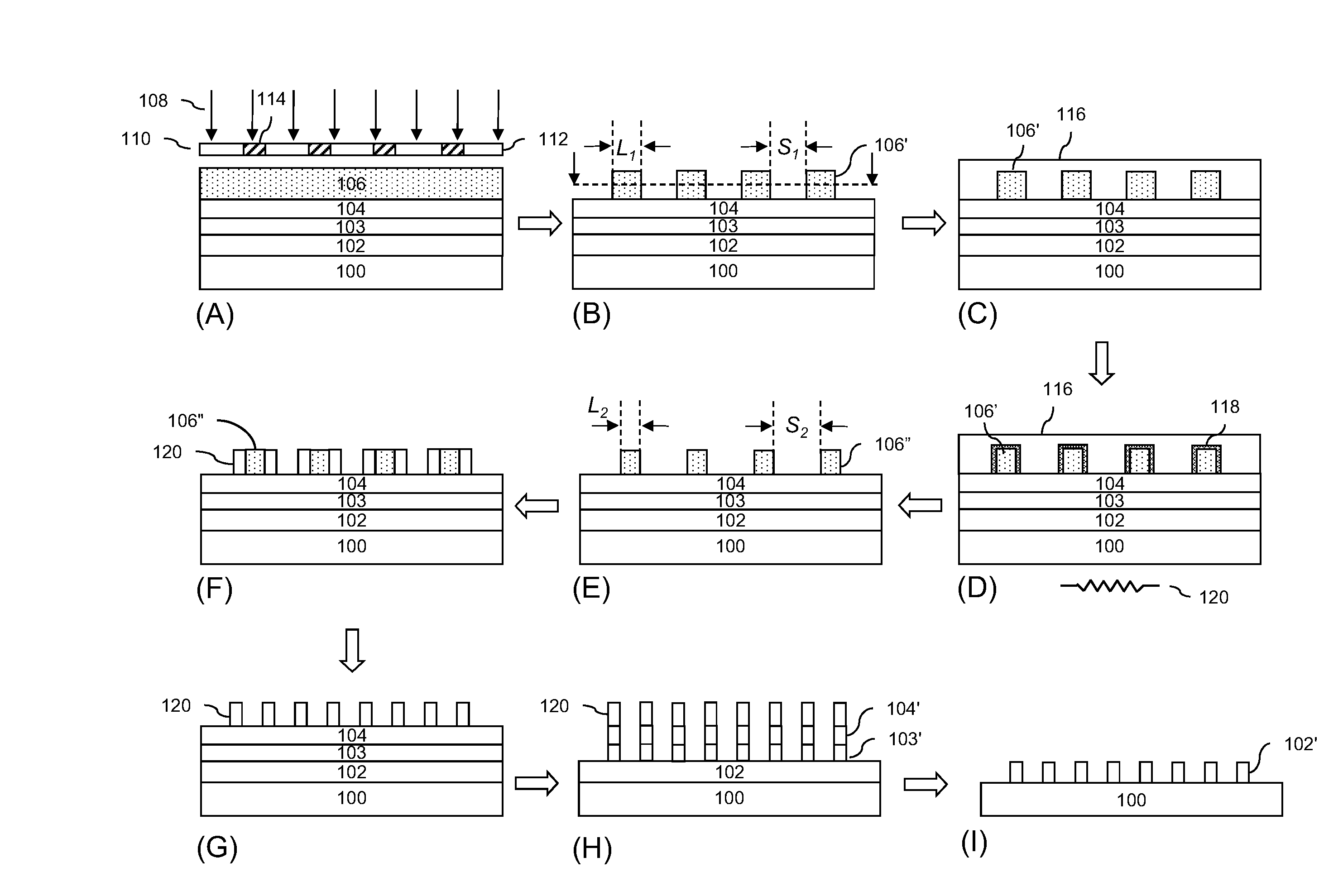
[0049]Photoresist A was spin-coated on an organic bottom antireflective coating (BARC AR™124 23 nm / AR™26N 77 nm (Rohm and Haas Electronic Materials LLC)) over 12 inch silicon wafers and softbaked (SB) at 95° C. for 60 seconds, to a thickness of 700 Å. Opticoat™ OC2000 topcoat material (Rohm and Haas Electronic Materials LLC) was coated on the resist to form an immersion topcoat layer. The coated wafers were exposed with an ASML ArF 1900i immersion scanner with NA=1.35, Dipole 35Y illumination (0.9 / 0.635sigma), plus x polarization, and post-exposure baked (PEB) at 90° C. for 60 seconds. The coated wafers were treated with 0.26N (normal) aqueous tetramethylammonium hydroxide solution to develop the imaged resist layers to form 45 nm 1:1 line and space resist patterns. Linewidth was measured for one of the patterned wafers. A 70 nm thick layer of the trimming composition of Example 1 (PTC 1) or Example 2 (PTC 2) was spin-coated over another of the patterned wafers, baked at the conditi...


PUM


Abstract

Provided are methods of trimming photoresist patterns. The methods involve coating a photoresist trimming composition over a photoresist pattern, wherein the trimming composition includes a matrix polymer, a thermal acid generator and a solvent, the trimming composition being free of cross-linking agents. The coated semiconductor substrate is heated to generate an acid in the trimming composition from the thermal acid generator, thereby causing a change in polarity of the matrix polymer in a surface region of the photoresist pattern. The photoresist pattern is contacted with a developing solution to remove the surface region of the photoresist pattern. The methods find particular applicability in the formation of very fine lithographic features in the manufacture of semiconductor devices.

Description

[0001]This application claims the benefit of priority under 35 U.S.C. §119(e) to U.S. Provisional Application No. 61 / 582,289, filed Dec. 31, 2011, the entire contents of which are incorporated herein by reference.BACKGROUND[0002]The invention relates generally to the manufacture of electronic devices. More specifically, this invention relates to methods of trimming photoresist patterns useful in shrink processes for the formation of fine lithographic patterns.[0003]In the semiconductor manufacturing industry, photoresist materials are used for transferring an image to one or more underlying layers, such as metal, semiconductor and dielectric layers, disposed on a semiconductor substrate, as well as to the substrate itself. To increase the integration density of semiconductor devices and allow for the formation of structures having dimensions in the nanometer range, photoresists and photolithography processing tools having high-resolution capabilities have been and continue to be dev...

Claims


Application Information

Patent Timeline
Patent Type & Authority Applications(United States)
IPC IPC(8): H01L21/308
CPCH01L21/0274G03F7/405G03F7/0392H01L21/308G03F7/40H01L21/0273
Inventor XU, CHENG-BAI
Owner ROHM & HAAS ELECTRONICS MATERIALS LLC
Why Eureka
Try Eureka