Silicon Heterojunction Solar Cells

a solar cell and heterojunction technology, applied in the field of solar cells, can solve the problems of more long wavelength infrared radiation, far from what may theoretically be achieved, and achieve the effect of enhancing device performance and cost of manufacturing and performance advantages

Inactive Publication Date: 2013-07-18
SVAGOS TECHNICK INC
View PDF1 Cites 24 Cited by
  • Summary
  • Abstract
  • Description
  • Claims
  • Application Information

AI Technical Summary

Benefits of technology

[0008]Furthermore, the present invention includes device structures based on the HIT solar cell which are expected to provide cost of manufacturing and performance advantages. For example, embodiments of the present invention may include a solar cell device architecture compr...

Problems solved by technology

However, the fabrication by mechanical thinning and handling of these very thin wafers poses problems for manufacturing and is not economically viable—there is a need for improved methods of fabricating and handling thin silicon in the production of HIT solar cells,
Furthermore, as silicon wafer thickness is reduced to reduce silicon consumption and hence manufacturing costs of photovo...

Method used


Image

  • Silicon Heterojunction Solar Cells
  • Silicon Heterojunction Solar Cells
  • Silicon Heterojunction Solar Cells

Examples


Embodiment Construction

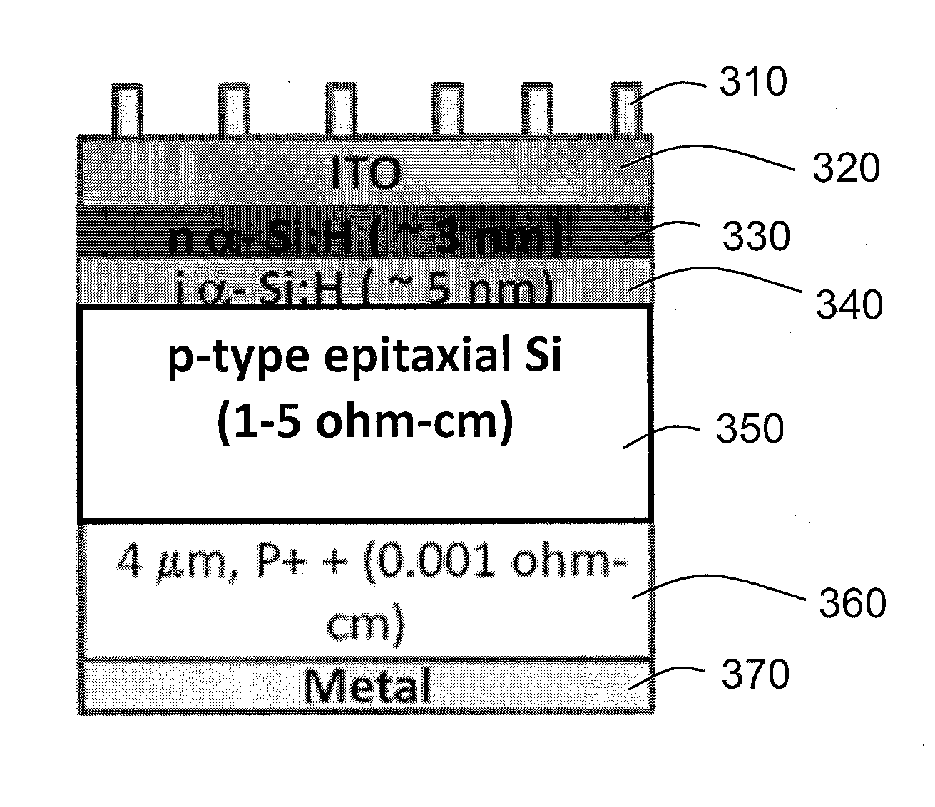
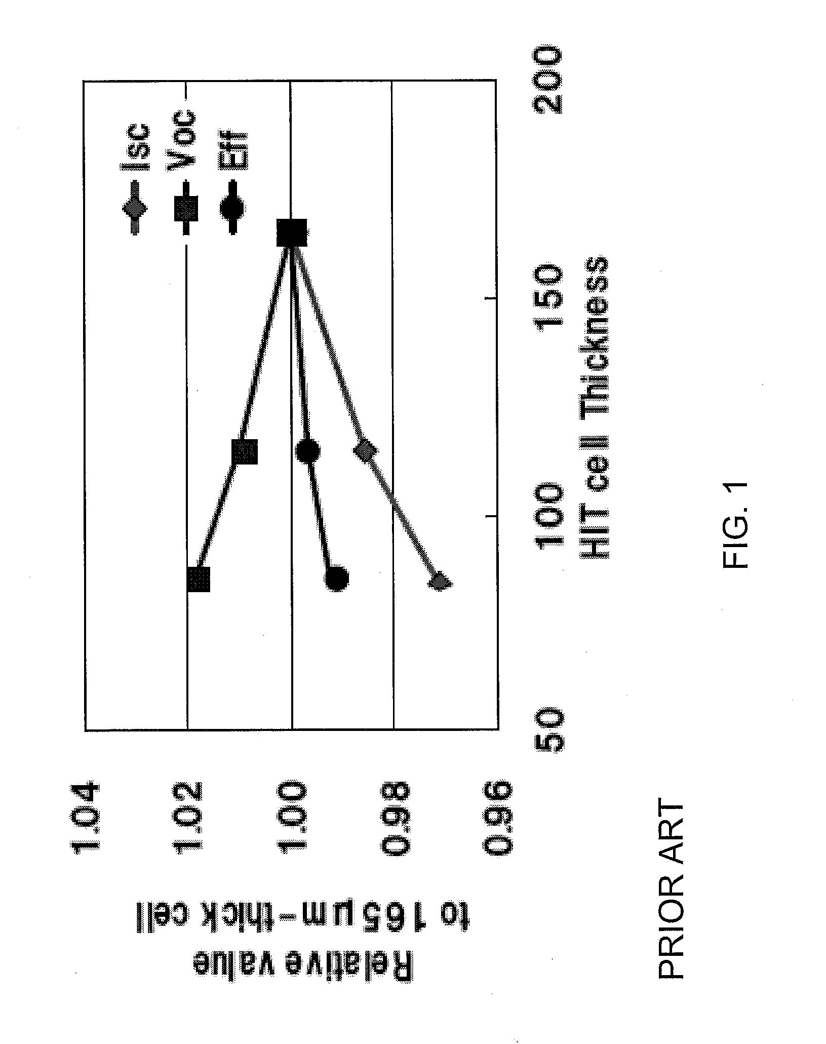
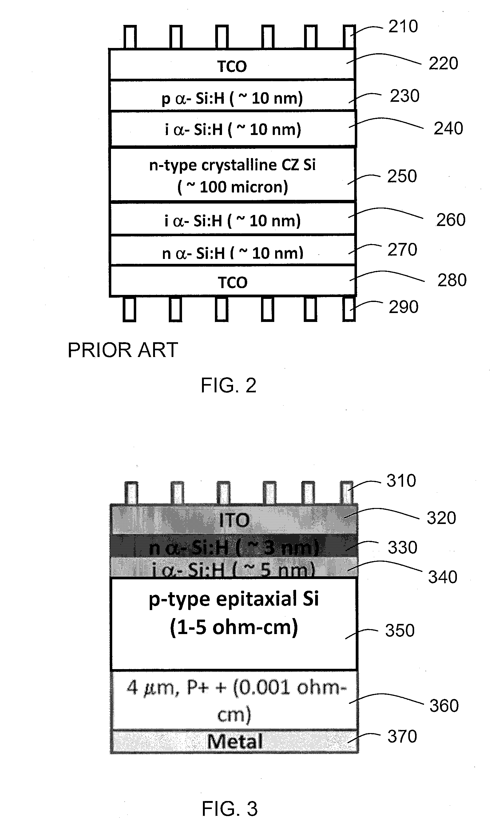
[0021]Embodiments of the present invention will now be described in detail with reference to the drawings, which are provided as illustrative examples of the invention so as to enable those skilled in the art to practice the invention. Notably, the figures and examples below are not meant to limit the scope of the present invention to a single embodiment, but other embodiments are possible by way of interchange of some or all of the described or illustrated elements. Moreover, where certain elements of the present invention can be partially or fully implemented using known components, only those portions of such known components that are necessary for an understanding of the present invention will be described, and detailed descriptions of other portions of such known components will be omitted so as not to obscure the invention. In the present specification, an embodiment showing a singular component should not be considered limiting; rather, the invention is intended to encompass ...


PUM


Abstract

Methods are described for fabricating HIT solar cells, including double heterojunction and hybrid heterojunction-homojunction solar cells, with very thin single crystal silicon wafers, where the silicon wafer may be less than 80 microns thick, and even less than 50 microns thick. The methods overcome potential issues with handling these very thin wafers by using a process including epitaxial silicon deposition on a growth substrate, partial cell fabrication, attachment to a support substrate and then separation from the growth substrate. Some embodiments of the present invention may include a solar cell device architecture comprising the combination of a heterostructure on the front side of the device with a homojunction at the rear of the device. Furthermore, device performance may be enhanced by including a dielectric stack on the backside of the device for reflecting long wavelength infrared radiation.

Description

CROSS-REFERENCE TO RELATED APPLICATIONS[0001]This application claims the benefit of U.S. Provisional Application No. 61 / 586,701 filed Jan. 13, 2012, and U.S. Provisional Application No. 61 / 656,957 filed Jun. 7, 2012, both incorporated herein by reference in their entirety.FIELD OF THE INVENTION[0002]The present invention relates generally to solar cells, and more particularly to silicon heterojunction solar cells with high efficiency.BACKGROUND[0003]The fabrication of a Heterojunction with Intrinsic Thin-layer (HIT) device, including a thin (˜10 nm) amorphous silicon film on a single crystal substrate, has been shown to enable solar cells with high open circuit voltages, as a result of the larger band offset achieved between the wider band gap amorphous silicon and the single crystal silicon as well as the superior surface passivation characteristics of amorphous silicon. (M. Taguchi et al., Proceedings 5th Photovoltaic Science and Engineering Conference (1990) 689). Recent research...

Claims


Application Information

Patent Timeline
IPC IPC(8): H01L31/078H01L31/20
CPCH01L31/078H01L31/202H01L31/022425H01L31/056H01L31/1892Y02E10/52H01L31/0747H01L21/02513H01L21/02532H01L21/0245H01L21/02381H01L21/02502H01L21/3147H01L33/22
Inventor RAVI, KRAMADHATI V.
Owner SVAGOS TECHNICK INC
Why Eureka
Try Eureka